This thread has been locked.

If you have a related question, please click the "Ask a related question" button in the top right corner. The newly created question will be automatically linked to this question.

TINA/Spice/ADS1298: ADS1298

Part Number: ADS1298
Other Parts Discussed in Thread: TINA-TI,

Tool/software: TINA-TI or Spice Models

Greetings Alex,

Thank you for your continuous support. 

I am having a difficult time to make the ADS1298 work. I have tried to look for similar thread but no luck so far. 

To start with, I can read the register ID and be able to read /write. When I used the internal test signal, it was initially noisy but I found out that the noise is not from the ADS instead it was related the arduino baud rate. Then Somehow I got a clean square wave for the 8 channels and attached is the picture. 

I hope I am reading the test signals right. 

Then When I have tried to read the ECG signal from two channels, channel 2 and 3 the signal does not look like ECG at all. My configurations are as follows.

// Boot sequence

// Issue Reset Pulse
digitalWrite(PIN_RESET, HIGH);
delay(1000);
digitalWrite(PIN_RESET, LOW);
delay(1000);
digitalWrite(PIN_RESET, HIGH);
delay(100);

// Reset communication
digitalWrite(PIN_CS, LOW);
delay(100);
digitalWrite(PIN_CS, HIGH);

// Wait longer for TI chip to start
delay(500);

// Send SDATAC Command (Stop Read Data Continuously mode)
writeCommand(SDATAC);
delay(10);

// Set ADC to work at high resolution 0.5KS/sampling rate, HP,multiple read back, clken-0,
//write(CONFIG1, 0xC6);//
write(CONFIG1, 0x45);//500SPS, LP, multiple read back, clken =0
// Generate internal test signal
write(CONFIG2, 0x10);//variable chopping frequency, internal test src, 2* test amp and test frequ of 01.
//write(CONFIG4, 0x02);
// reference buffer, 2.4Vref, reld mes- open, rldRef - internal, rld buf-on, rld sens-enabled, rld lead off-connected
write(CONFIG3, 0xCE);
write(LOFF, 0x41);//90%, current mode, 6nA, ac lead-off detection

write(RLD_SENSP, 0x03);// channel three 
write(RLD_SENSN, 0x03);
write(LOFF_SENSP, 0x03);
write(LOFF_SENSN, 0x03);
write(LOFF_FLIP, 0x00);//no flip
// All GPIO set to output 0x0000: 
write(GPIO, 0x00);

//Willson terminals
write(WCT1, 0x0B); // WCTA powered and connected to channel 2 negative input
write(WCT2, 0xC4); // WCTB connected to channel 2 positive input and WCTC connected to channel 3 positive input


//Pace and respiration disabled
write(PACE, 0x00); // pace disabled
write(RESP, 0x00); // respiration disabled

write(CONFIG4, 0x02);//Turn on DC lead off comparator
//CONFIG4, LOFF_SENSP, LOFF_SENSN, LOFF_FLIP, LOFF_STATP, LOFF_STATN

write(CH1SET, 0x81);// turn off channel one
write(CH2SET, 0x20);// Set channel two - lead one as differential input with x2 gain - LA and RA
write(CH3SET, 0x20);// Set channel three - lead two as differential input with x2 gain - LL and RA

for (int i = 4; i <= 8; i++) {// turn down the rest of the channels and shorted
write(CHnSET + i, 0x81);
//write_byte(CHnSET + i, 0x15);
}

// put the ADS back to read data continuous mode
writeCommand(RDATAC); 

//Set the start pin high 

digitalWrite(PIN_START, HIGH);
delayMicroseconds(10);

After the 50Hz notch filter the signal still does not look like ECG at all. 

What do you think I missed here?? Register configuration, channel set ?? I would appreciate any help.

KInd regards!!

  • Hello Mes,

    Most of the team is out on US holiday. We'll get back to you the week of 11/26.
  • Hey Collin,

    Thanks and wish you and the rest of the team members a lovely thanksgiving.  

    In the meantime I have more questions. 

    1. When the ADS is powered up from a single ended 5V supply (AVDD = +5V, AVSS = 0V), is it possible to use the ads in differential mode?? Like the positive input of channel 2 is connected to RA and the negative is connected to LA to measure ECG. 

    2. Could you please go through my schematics attached as pdf and tell me why my pcb is not working? 

    ECG_Schematics.pdf

    3. Regarding the SPI connection, I have powered up the ads from 3.3V (DVDD = 3.3V)  and when I tried to communicate with a 3.3V microcontroller, I could not make it work. Instead, when I connect the ads with arduino uno with out logic shifter I could be able to read the registers and the test signals as attached in my previous question. The problem is using the oscilloscope, I found out there is about 1Vpp noise right the top of the clock and DRDY signal. Assuming that is the noise from the voltage difference between the 5V arduino spi and the 3.3ads spi lines, I tried to use voltage divider and fed the 3.3V to the ads side of the spi line. But the previous problem I have with the 3.3V microcontroller comes and I could not read the ads registers at all. If the AVDD is +5 Vand DVDD is 3.3V my assumption is the ads SPI line works at 3.3V. Am I wrong or is there something I missed here??

    Thanks and looking forward to hear from you!

    Mes


  • Hi Mes!

    Thanks for the Thanksgiving wishes, it was indeed lovely!

    I think that there may be an issue with your WCT register settings. Your code comments say "WCTB connected to channel 2 positive input and WCTC connected to channel 3 positive input" After writing C4h = 11000100b, you are actually connecting WCTB to Ch1P and WCTC to Ch3P. Ch1 is turned off. Try writing D4h instead. 

    I went ahead and tried to answer your questions and provide some follow up steps if above does not help. Let me know.

    1) Yes
    2) At first pass I do not see any schematic issues.
    3) Can you post an oscilloscope shot showing this noise at the top of the CLK & DRDY signals?

    Can you also clarify the test cases below? I'm having trouble following exactly what you're looking at here.

    - ADS @ 3.3V to uC @ 3.3V - no function
    - ADS @ 3.3V to Arduino 5V (then level shifting from 5V to 3.3V to uC) - function
    - Not sure what you mean about feeding 3.3V to the ADS side of spi line.

    Your assumption is correct. The 3.3V SPI output level of the ADS should be able to directly interface with the 3.3V MCU.

    Is it possible that the level shifter is being used unknowingly/incorrectly for the first case which causes an improper voltage level at the uC? I recommend following the SPI line using an oscilloscope to try to identify the source of the noise and to make sure that communication is being done at the proper voltage level. Unfortunately I am not familiar with the Arduino products so I cannot help too much.

    Probe your power supplies and reference to make sure they are clean.

  •  Dear alex,

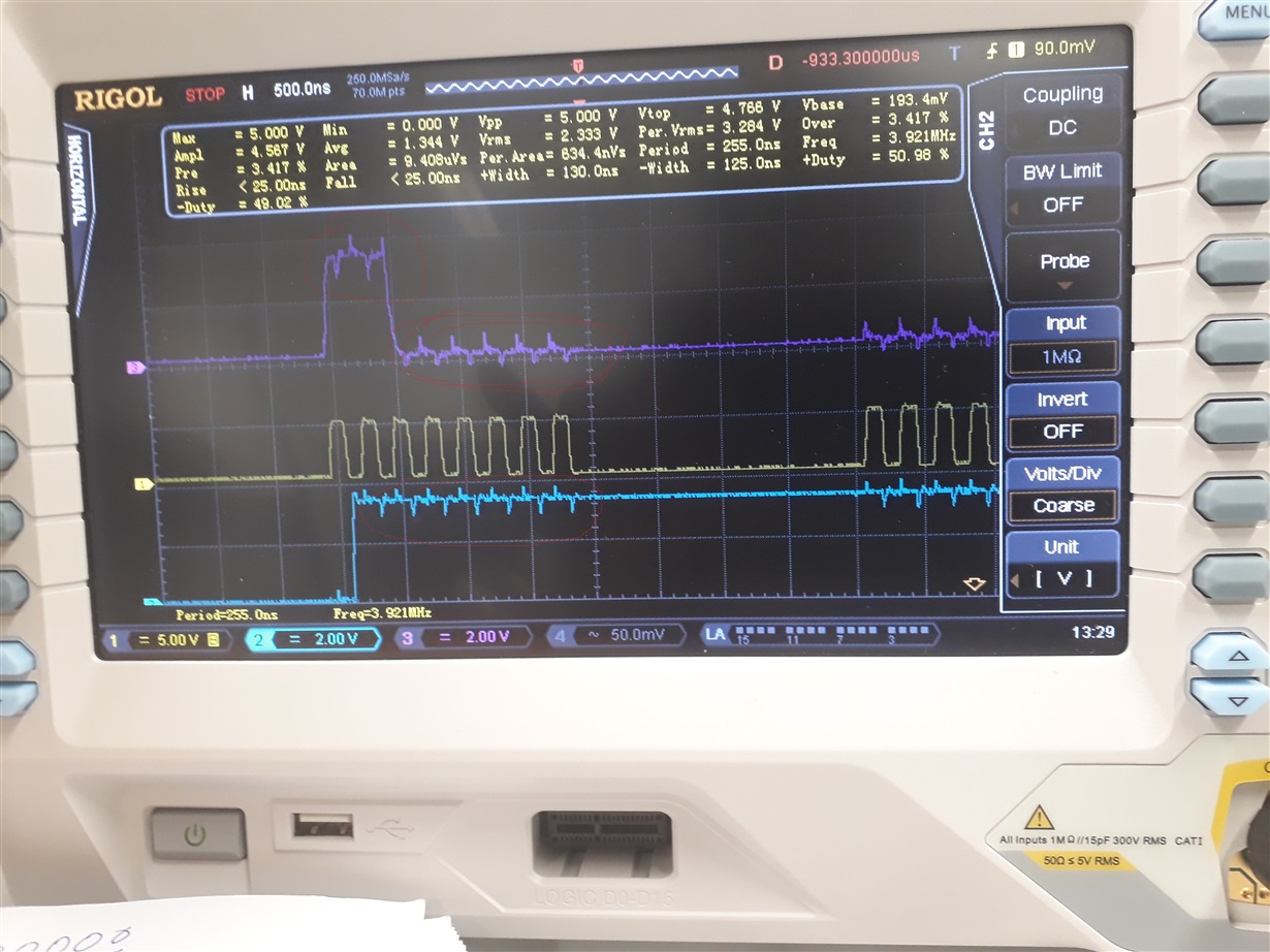
    Welcome back and thank you very much for your detailed explanation.  I have tried to attach oscilloscope image regarding the  overshot of the values. CH3- Data out from ADS, CH1- (yellow-middle) - CLOCK and CH2- DRDY. as you can see the voltage is above 4 volts while in principle it should be below 4 (around 3.3v). Additionally, the following figure is from the internal test signal. Does it look like the test signal or I am reading a random noise??

    Your comments will be appreciated. 

    Kind regards!!     

  • Hi Mes,

    It looks like your clock signal is nearly 5V - that's too high if you're using DVDD of 3.3V. The absolute maximum rating for digital inputs is DVDD + 0.3. If you have been applying 5V signals with DVDD = 3.3V, then your device may be damaged.

    Review the timing settings in the 7.6 Timing Requirements: Serial Interface section.

    The test signal looks fine, but it is difficult to know without understanding what the axis scale is.
  • Dear Alex,

    I thank you very much. You are right that is my assumption too. The SPI line / digital lines of the ADS might be toasted and that is why I am really getting a difficult time getting it work. Do you think it is still possible to read from and write to the registers even if the pins are some how shaky/ broken?? I am reading the ADS ID value and be able to write to the registers. Apart from the register values, I could not be able to read any thing. Either I read a constant values or random noise that does not look like ECG at all.

    I have ordered one more ADS chip from mouser and hope will get it by next monday or tuesday. This time I will be more careful and will keep you posted. In the meantime I am still waiting the new ADS user manual from you.


    Kind regards
    Mes
  • Hi Mes,

    Happy to help! Unfortunately if the pins are broken it is probably not possible to read/write to the device. I'll ask a colleague and see what he thinks.

    I'm glad that you remembered the new user manual! I've been busy working on other things, but I'm hoping to work on it a lot towards the end of this month.
  • Dear Alex,

    Thanks for your continuous support. Unfortunately my order has been delayed and I have not received the ADS chip. It feels like the chip has been dancing in the US for three days and landed in China a couple of hours a go.

    Again I was expecting the info on whether it is possible to read/write the registers values if the SPI lines are toasted??

    Again I have the following values:
    Vvcap1 = 1.19V - - - - - - OKAY
    Vvcap2 = 2.51V - - - - - - - OKAY for 5V supply
    Vvcap3 = 6.89V - - - - - - - - OKAY for 5V supply
    Vcap4 = 1.19V - - - - - - - - New and seems it is shorted to Vvcap1 as it exactly mirrors the value at Vvcap1

    Any time the value at Vvcap1 is changed to like 1.18V the voltage at the Vvcap4 reads 1.8V too.

    Based on the above values, do you think the Vcap4 pin / Vcap1 pin broken??

    Again thanks and looking forward to hear from you.

    Mes!
  • Hi Mes,

    Did you ever change the WCT register to D4h? I didn't receive confirmation from you.
    VCAP4 is for the reference, so you can try changing the reference voltage to see if it changes.
    I chatted with a colleague of mine and unless the SPI driver for the uC is very strong, the device should be ok.
  • Dear Alex,

    I thank you very much for your continuous support. I have already changed the WCT register to D4h. However nothing is changed. 

    My register values are as follows:

                      //  Boot sequence 

    // Issue Reset Pulse
    digitalWrite(PIN_RESET, HIGH);
    delay(1000);
    digitalWrite(PIN_RESET, LOW);
    delay(1000);
    digitalWrite(PIN_RESET, HIGH);
    delay(100);

    // Reset communication
    digitalWrite(PIN_CS, LOW);
    delay(100);
    digitalWrite(PIN_CS, HIGH);

    // Wait longer for TI chip to start
    delay(500);

    // Send SDATAC Command (Stop Read Data Continuously mode)
    command(SDATAC);
    delay(10);

    // Set ADC to work at high resolution 0.5KS/sampling rate, HP,multiple read back, clken-0,
    write(CONFIG1, 0xC6);//
    // Generate internal test signal
    write(CONFIG2, 0x10);//Activate a (1mV ´ V /2.4) Square-Wave Test Signal
    write(CONFIG3, 0xCE);// reference buffer, 2.4Vref, rld mes - open, rldRef - internal, rld buf-on, rld sens-enabled, rld lead off-conected
    delayMicroseconds(100); //Wait for Internal Reference to Settle

    write(LOFF, 0x41);//90%, current mode, 6nA, ac lead-off dectection
    write(RLD_SENSP, 0xFF); // all channels
    write(RLD_SENSN, 0x07);//
    write(LOFF_SENSP, 0xFF);//all channels
    write(LOFF_SENSN, 0x07);
    write(LOFF_FLIP, 0x00);//no flip
    write(GPIO, 0x00); // All GPIO set to output 0x0000: (floating CMOS inputs can flicker on and off, creating noise)

    //Willson terminals
    write(WCT1, 0x0B); // WCTA powered and connected to channel 2 negative input
    write(WCT2, 0xD4); // WCTB connected to channel 2 positive input and WCTC connected to channel 3 positive input
    //Pace and respiration disabled
    write(PACE, 0x00); // pace disabled
    write(RESP, 0x00); // respiration disabled

    write(CONFIG4, 0x02);//Turn on DC lead off comparator

                   for (int i = 1; i <= 8; i++) {
                               write(CHnSET + i, 0x60);
                    }

    // put the ADS back to read data continuous mode
    command(RDATAC); // can't read registers in rdatac mode!

    // Toggle the Start pin to HIGH before exit the ads setup
    digitalWrite(PIN_START, HIGH);
    delay(150);

    Regarding the Vvcap4 value, even if I change the reference voltage to 4V I am reading the same 1.9V. Based on your comment above it is supposed to change to what value?? I have done everything possible and I have no idea what I could change. My only option is to assemble a new board and see the if the ads is damaged or not. Unfortunately the supplier is really awful and could not keep the promised delivery day. I was expecting the ads on last Tuesday. But I have not received it yet and from the tracking number it seems the new delivery day is not available. 

    Again thank you and looking forward to hear from you.

    Kind regards

    Mes!!

  • Hi Mes,

    VCAP4 is supposed to be mid reference. In your previous post you said VCAP4 - 1.19V, about half of 2.4, and now you say it is 1.9V for a 4V reference, also about half. Since all of your VCAP values are in tact, this is good news.

    I recommend you review the initial flow at power up, figure 93. in the datasheet to make sure that everything is being configured correctly. After you set CLKSEL =1, does the oscillator correctly wake up? Does /DRDY toggle? Do you set /PDWN and /RESET = 1 and wait tPOR? Does VCAP reach 1.1V? Do you issue an additional /RESET and wait for 18tCLK?
  •      Ch2            Ch3      Ch4            Ch5            Ch6              ch7            ch8         ch1              

    Dear Alex,

    Again thank you for your valuable feedback. To make sure all of your comments:set CLKSEL =1, does the oscillator correctly wake up? Does /DRDY toggle? Do you set /PDWN and /RESET = 1 and wait tPOR? Does VCAP reach 1.1V? Do you issue an additional /RESET and wait for 18tCLK?

    CLKSEL = 1; the oscillator wakes up and the /DDRY toggles. /PDWN = RESET = 1, I have waited for tPOR but is there a maximum value?? The following is my Boot sequence.

    // Boot sequence

      // Issue Reset Pulse

       digitalWrite(PIN_RESET, HIGH);

       delay(500);// Wait for Min(tpor) = tclk * 2^18 = 1/2.048mHz*2^18 = 128ms - for power on rest and oscillator Start-up

       digitalWrite(PIN_RESET, LOW);

       delay(500);

       digitalWrite(PIN_RESET, HIGH);

       delay(500); //Wait for 18tclk

       // Reset communication

       digitalWrite(PIN_CS, LOW);

       delay(10);// Delay 10 ms

       digitalWrite(PIN_CS, HIGH);

       delayMicroseconds(10); // Delay 10 ms

       // Send SDATAC Command (Stop Read Data Continuously mode)

       command(SDATAC);

    Vcap reaches 1.1V, VREV+ - VREF- = 2.4V / 4V for 4 voltage reference

    My regester settings are as follows:

       write(CONFIG3,  0xCE);// reference buffer, 2.4Vref, rld mes - open, rldRef - internal, rld buf-on, rld sens-enabled, rld lead off-connected

       delayMicroseconds(100); //Wait for Internal Reference to Settle

       // Set ADC to work at high resolution 0.5KS/sampling rate, HP,multiple read back, clken-0,

       write(CONFIG1,   0xC6);//

       // Generate internal test signal

       write(CONFIG2, 0x10);//Activate a (1mV ´ V /2.4) Square-Wave Test Signal

       write(LOFF,       0x41);//90%, current mode, 6nA, ac lead-off dectection

       write(RLD_SENSP,  0x06); // channels 2&3  

       write(RLD_SENSN,  0x06);//channels 2&3

       write(LOFF_SENSP, 0x06);//channels 2&3

       write(LOFF_SENSN, 0x06);//channels 2&3

       write(LOFF_FLIP,  0x00);//no flip

       write(GPIO,       0x00); // All GPIO set to output 0x0000: (floating CMOS inputs can flicker on and off, creating noise)

       //Willson terminals

       write(WCT1, 0x0B); // WCTA powered and connected to channel 2 negative input

       write(WCT2, 0xD4); // WCTB connected to channel 2 positive input and WCTC connected to channel 3 positive input

       //Pace and respiration disabled

       write(PACE, 0x00); // pace disabled

       write(RESP, 0x00); // respiration  disabled

       write(CONFIG4, 0x02);//Turn on DC lead off comparator

       //CONFIG4, LOFF_SENSP, LOFF_SENSN, LOFF_FLIP, LOFF_STATP, LOFF_STATN

       for (int i = 1; i <= 8; i++) {

        //write(CHnSET + i, 0x00);//Gain 6 and normal input electrode

        write(CHnSET + i, 0x35);// Internal test signal gain = 3x

        //write(CHnSET + i, 0x31);//Gain 3 and all channels shorted

       }

    Then for the internal short signal the optimal setup seems 2.4V reference and 3x / 4x gain with a maximum noise of 505uV from CH6. Attached is some snapshots.  

    For the internal test signal, I kind of get a clean square signal but the amplitude is (4000*2.4/(2^23-1) * 1/3 = 0.381mV. I have connected the teste_pace_out1 and 2 to AGND. Do you think it affects the amplitude of the test signal?? Attached is the signal for 500 samples (just one cycle => (133110 - 132610) = 500 samples). 

    Everything seems working but when I tried to connect an electrode or a simulator the data is random and I can't get it work. Do you think I should assemble a another prototype??  Additionally, I have used the following formula to calculate the real values in Voltage. 

    if(dataValue (the 24 bit data ) >= 8388608 )){           // Check for  the maximum value, maximum positive value is 7FFFFF - hex or 8388607
    dataValue = dataValue  - 16777216;                         //[ dataPacket - 1 (in decimal)*LSB size]/gain, where LSB size = VREF/(2^23-1)   - in voltage  
    }

    Am I getting it right ??  If so what else should I do?? It really took me a lot to figure out the problem. I have an ECG AFE from discrete components and INOP and it is working but the ads chip isn't.  I am really confused.

    Waiting for your usual feedback. 

    Kind regards

    Mes

  • Hi Mes,

    There is not a maximum time for tPOR, you just need to make sure that you wait at least the minimum time or until VCAP1 is greater than or equal to 1.1V, whichever is longer.

    Try removing this line:

    digitalWrite(PIN_CS, HIGH);

    From figure 93.:
    // Activate DUT
    // /CS can be Either Tied Permanently Low
    // Or Selectively Pulled Low Before Sending
    // Commands or Reading/Sending Data from/to Device

    You're pulling /CS high again before sending the SDATAC command.

    One last thing, not sure if this was intentional or not, but you write a 10uS delay, comment is 10mS.
    delayMicroseconds(10); // Delay 10 ms

  • Hey Alex,

    Great to hear from you as usual. I left out the digitalWrite(PIN_CS, HIGH); in case it makes difference as I have pulled low the /CS inside of the write function. Could you comment on my formula to calculate the real values? 

    if(dataValue (the 24 bit data ) >= 8388608 )){           // Check for  the maximum value, maximum positive value is 7FFFFF - hex or 8388607 

    dataValue = dataValue  - 16777216;                         //[ datgaValue - 1 (in decimal)*LSB size]/gain, where LSB size = VREF/(2^23-1)   - in voltage  

    }

    Again the noise value especially on two of the channels. 

    Kind regards!

    Mes

  • Hi Mes,

    Happy to help!

    Ah I see, I didn't know that you built it into the write function.

    //[ datgaValue - 1 (in decimal)*LSB size]/gain, where LSB size = VREF/(2^23-1) - in voltage
    is technically incorrect since the LSB size will be multiplied by 1 before getting subtracted from the dataValue.

    It should be this: (Code (decimal) - 1) x LSB / Gain = Volts

    e2e.ti.com/.../1363393