This thread has been locked.

If you have a related question, please click the "Ask a related question" button in the top right corner. The newly created question will be automatically linked to this question.

ADS54J60EVM: Shifting the phase of the ADC clock in very small steps of 25 ps

Part Number: ADS54J60EVM
Other Parts Discussed in Thread: ADS54J60, LMK04828, , ADS54J69

We are currently evaluating the ADS54J60 for a project and need the possibility to move the sampling phase of the ADC relative to the FPGA (there are several ADCs, each with an individual sampling delay).

The ADC data is sampled at 500 MSa/s @ 16 bit = 8 Gbit/s => using 8B/10B of JESD204B ends up to be 10 GSa/s and routed to an ZCU102 Board of Xilinx on the FMC connector routed to the Zynq Ultrascale+ MPSoC FPGA.

I see the system working properly and check the data from the ADC using an integrated logic analyzer (ILA) of Xilinx and see clean and proper data.

Now I start moving on the eval board the clock distribution chip  LMK04828, the output DCLK 2, the analog delay, in steps of 25 ps. I'm able to observe the phase shift with an oscilloscope between the reference clock and the recovered clock from the FPGA... hence  this part is working as it should.

At about 950 ps analog delay the FPGA is not able to lock anymore on the ADC data and delivers lots of crap. Will say not even the K28.5 is sampled anymore correctly.

Now my question_ Did anyone ever try to move the sampling phase of the ADC successfully using the JESD204B interface? In theory this should be possible, since the FPGA MGTs run with slightly different frequencies hence I would have expected that it is as well possible with a JESD204B... especially since I'm only sending K25.5 characters which is used to align the symbols.

Cheers

Goran

  • Goran,

    DCLK2 is the ADC clock. What is the reference clock you are referring to when looking with an oscilloscope? Is this the ADC clock or the FPGA reference clock which is from DCLK0? Per the standard the device clock and SYSREF have to meet setup and hold at both locations. If you are moving the ADC clock only, the timing of SYSREF inside the ADC will eventually become invalid. The FPGA is counting on this timing to be stable to keep both clock domains synchronized. If you are using multiple ADC's and subclass 1, all the data should all be aligned when it comes out of the JESD block on the FPGA side. I have not seen any customers attempt what you are trying to do.

    Regards,

    Jim

  • Hello Jim,

    Yes, on the ADS54J60EVM eval board the DCLK2 is the output on the LMK04828 which drives the ADC device clock running at 1 GHz. This is how TI did their eval board.

    The so called "reference clock" is the 250 MHz device clock of the FPGA... if you use the terms of JESD204B standard... or if you like to use the terms defined by Xilinx then you call it reference clock of the multi gigabit transceiver... sorry, I'm a FPGA developer and tend to use the terms from my garden.

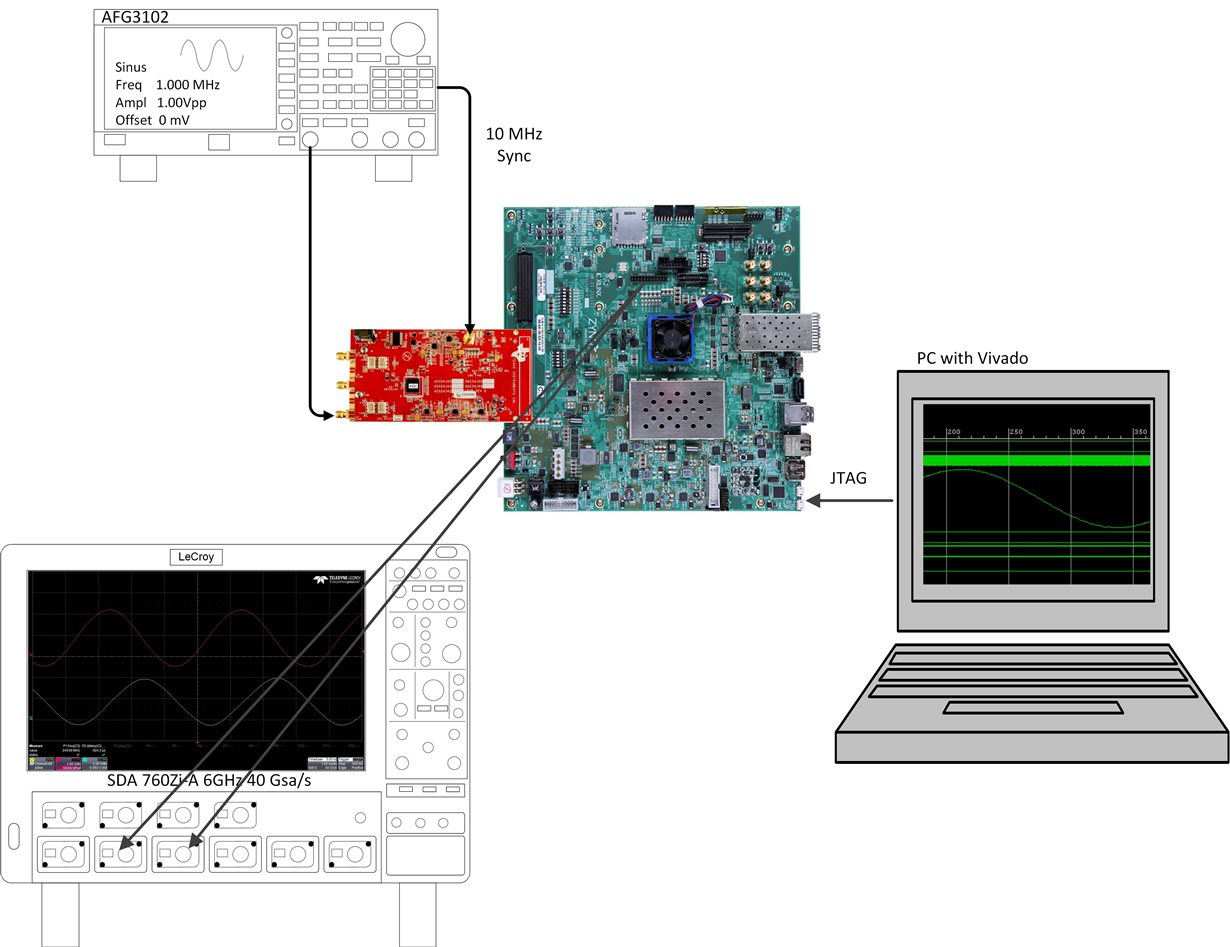
    Since these multi gigabit transceivers have a clock/data recovery, you will get the recovered clock from the FPGA as well. These two clocks I routed to an digital output on my Xilinx ZCU102 evaluation board and measure the 250 MHz device clock on the FPGA with the recovered 250 MHz clock  using a fast scope from LeCroy (the SDA 760Zi-A using 40 GSa/s). I attached a picture of my setup.

    Since the SYSREF is only used at the beginning  of the JESD204B protocol in order to synchronize internal framing in both the transmitter and receiver, I switched it off after reaching sync by powering down of the LMK04828 output SDCLKOUT3 which is the SYSREF on the ADS54J60EVM eval board. Since the SYSREF is switched off when I do the analog delay of the device clock of the ADC I guess the setup/hold time is irrelevant.

  • Some more infos concerning the drawing:
    If you zoom closer you see in the oscilloscope a print screen of my measurement and on the laptop the sinus sampled and retrieved directly after the multi gigabit transceiver by an integrated logic analyzer.
  • Goran,

    Even though you turned off SYSREF, in theory, both clock domains or LMFC's are locked and referenced to each other. This is no longer true when you start moving the ADC clock phase. Eventually the serdes data out of the ADC will no longer line up wit the reference clock sent to the FPGA form the LMK.

    Why may I ask, are you doing this adjustment?

    Regards,

    Jim 

  • Hello Jim,

    Concerning you remark: "... both clock domains or LMFC's are locked and referenced to each other. ... " this is only true if you use the device clock to operate your LMFC. However, the FPGAs use the recovered clock for their LMFC counting and hence the two LMFCs stay synced. Remember there is a clock-data recovery in every multi gigabit transceiver. This clock-data recovery is the reason why FPGAs running at several Gigabit do NOT loose sync although they use individual oscillators (which are close in frequency, but never the same -> the phase changes slowly over the time). In our case here, the only thing which changes is the phase at the ADC in very small steps (so the clock-data recovery compensates for the phase shift) which I can as well observe when comparing the two clocks.
    Concerning: "...Why may I ask, are you doing this adjustment?... "
    We want to be able to adjust the sampling point which changes due to drift (temperature, humidity, aging, and so on) in sub nano second range. The measurement devices we build are extremely precise and we see this drifts.

    Cheers
    Goran
  • Goran,

    I agree with you but I still think there is a limit in which you can make this adjustment. Have you tried to re-initialize the JESD link after the data went bad? Is there a chance you are overflowing the elastic buffer in the FPGA? Is your RBD value set to the max (RBD = K)?  Does increasing the value of "K" help?  Have you tried contacting Xilinx regarding this issue?

    Regards,

    Jim

  • Hello Jim,

    And here my answers:

    >"I agree with you but I still think there is a limit in which you can make this adjustment."
    As long as the phase change steps are very small (25 ps < 100 ps (bit-period of 10 Gbit/s)) and the various PLLs do not jump out of lock, I should be safe.

    >"Have you tried to re-initialize the JESD link after the data went bad?"
    Yes, I did this and it works properly if the analog delay is below 950 ps. Above 950 ps analog delay, the multi gigabit tranceiver does not lock anymore. Above 950 ps: When I send constantly K28.5, I see every now and then crappy data from the multi gigabit tranceiver.

    >"Is there a chance you are overflowing the elastic buffer in the FPGA?"
    Since the ADC and FPGA use the same clock source, the elastic buffer is not able neither to overflow nor to underflow. Or how would the elastic buffer change it's fill level if you read and write with exactly the same clock? This is only possible in the hypothetic case if your elastic buffer stores only one single value... hence if you have no elastic buffer at all.

    >"Is your RBD value set to the max (RBD = K)?"
    If you refer as RBD = "Rx Buffer Delay". The receive buffer is set to 64 octets, which are 16 frames in my configuration. However I look at the data directly after the multi gigabit tranceiver... the buffer is in the next stage the JESD204B core. Hence not relevant for my problem.

    >"Does increasing the value of "K" help?"
    The frame per multi-frame is set to 16 in my case to keep the latency low. But why should this make a difference when I constantly send K28.5?

    >"Have you tried contacting Xilinx regarding this issue?"
    Not yet, since the FPGA works stable if the analog delay is below 950 ps for the LMK04828 clock distribution chip. I guess the Xilinx folks will ask me exactly this.

    Question to you: TI uses an ALTERA/INTEL FPGA board for test purposes... could you reproduce what I wrote in all my previous logs?

    Regards,

    Goran
  • Bandwidth is kind of limited. Can you send the configuration file used to load the TI EVM for a pass case and failed case and I will give this a try with our TSW14J56EVM (Arria V based).
  • Jim,

    Now I measured the clock at the resistor R32 which is the terminating resistor for the ADC device clock on the eval board... and when I set 950 ps in my software tool provided by TI:
    ADS54Jxx EVM GUI
    Version information: 1.6
    Build date: 05/20/2016
    the LMK04828 switches the clock output off! What the heck happens here?

    Cheers
    Goran

  • MG84_LMK04828_250MHz_3MHz90625_1000MHz_3MHz90625.cfg

    MG84_ADS54J69_500MSaps_LMFS_2242_config.cfg

    Looks like our two entries were almost at the same time.

    Here my configuration:

    1.) First load the configuration for the clock distribution chip.

    2.) Hard reset the ADC by SW1 on the eval board

    3.) Load the configuration for the ADC

    My two configuration files are at the end of this log... sorry for some reasons I was not able to attach them as files.

    Cheers

    Goran

    MG84_LMK04828_250MHz_3MHz90625_1000MHz_3MHz90625.cfg

    LMK04828
    0x000 0x10          // Register 0x000 RESET, SPI_3WIRE_DIS; bit(7) := RESET = '0' = Normal Operation, clears back to 0; bit(6:5) := not used = '00'; bit(4) := SPI_3WIRE_DIS = '1' =  3 Wire Mode disabled; bit(3:0) := not used = '0000'
    0x002 0x00          // Register 0x002 POWERDOWN; bit(7:1) := not used = '0000000'; bit(0) := POWERDOWN = '0' = Normal Operation
    0x100 0x0C          // DCLKout0  and SDCLKout1  Register 0x100 CLKoutX_Y_ODL, CLKoutX_Y_IDL, DCLKoutX_DIV; bit(7) := not used = '0'; bit(6) := CLKoutX_Y_ODL = '0' = Output drive level; bit(5) := CLKoutX_Y_IDL = '0' = Input drive level; bit(4:0) := DCLKoutX_DIV = '01100' = 12
    0x101 0x55          // DCLKout0  and SDCLKout1  Register 0x101 DCLKoutX_DDLY_CNTH, DCLKoutX_DDLY_CNTL; bit(7:4) := DCLKoutX_DDLY_CNTH = 5 clock cycles delay; bit(3:0) := DCLKoutX_DDLY_CNTL = 5 clock cycles delay
    0x103 0x00          // DCLKout0  and SDCLKout1  Register 0x103 DCLKoutX_ADLY, DCLKoutX_ADLY_MUX, DCLKout_MUX; bit(7:3) := DCLKoutX_ALDY = 0 = 0 * 25 ps analog delay; bit(2) := DCLKoutX_ADLY_MUX = '0' = Divided without duty cycle correction or half step.
    0x104 0x20          // DCLKout0  and SDCLKout1  Register 0x104 DCLKoutX_HS, SDCLKoutY_MUX, SDCLKoutY_DDLY, SDCLKoutY_HS; bit(7) := not used = '0'; bit(6) := DCLKoutX_HS = '0' = 0 cycles; bit(5) := SDCLKoutY_MUX = '1' = SYSREF output; bit(4:1) := SDCLKoutY_DDLY = '0000' = Bypass; bit(0) := SDCLKoutY_HS = '0' = 0 cycles
    0x105 0x00          // DCLKout0  and SDCLKout1  Register 0x105 SDCLKoutY_ADLY_EN, SDCLKoutY_ADLY; bit(7:5) := not used = '000'; bit(4) := SDCLKoutY_ADLY_EN = '0' = Disabled; bit(3:0) := SDCLKoutY_ADLY = '0000' = 0 ps
    0x106 0xF0          // DCLKout0  and SDCLKout1  Register 0x106 DCLKoutX_DDLY_PD, DCLKoutX_HSg_PD, DCLKout_ADLYg_PD, DCLKout_ADLY_PD, DCLKoutX_Y_PD, SDCLKoutY_DIS_MODE, SDCLKoutY_PD; bit(7) := DCLKoutX_DDLY_PD = '1' = Powerdown; bit(6) := DCLKoutX_HSg_PD = 1' = Powerdown; bit(5) := DCLKoutX_ADLYg_PD = '1' = Powerdown; bit(4) := DCLKoutX_ADLY_PD = '1' = Powerdown; bit(3) := CLKoutX_Y_PD = '0' = Enabled; bit(2:1) := SDCLKoutY_DIS_MODE = '00' = Active in normal operation; bit(0) := SDCLKoutY_PD = '0' = Enable
    0x107 0x11          // DCLKout0  and SDCLKout1  Register 0x107 SDCLKoutY_POL, SDCLKoutY_FMT, DCLKoutX_POL, DCLKoutX_FMT; bit(7) := SDCLKoutY_POL = '0' = Normal; bit(6:4) := SDCLKoutY_FMT = '001 = LVDS ; bit(3) := DCLKoutX_POL = '0' = Normal; bit(2:0) := DCLKoutX_FMT = '001' = LVDS
    0x108 0x63          // DCLKout2  and SDCLKout3  Register 0x108 CLKoutX_Y_ODL, CLKoutX_Y_IDL, DCLKoutX_DIV; bit(7) := not used = '0'; bit(6) := CLKoutX_Y_ODL = '1' = Output drive level; bit(5) := CLKoutX_Y_IDL = '1' = Input drive level; bit(4:0) := DCLKoutX_DIV = '00011' = 3
    0x109 0x55          // DCLKout2  and SDCLKout3  Register 0x109 DCLKoutX_DDLY_CNTH, DCLKoutX_DDLY_CNTL; bit(7:4) := DCLKoutX_DDLY_CNTH = 5 clock cycles delay; bit(3:0) := DCLKoutX_DDLY_CNTL = 5 clock cycles delay
    0x10B 0x00          // DCLKout2  and SDCLKout3  Register 0x10B DCLKoutX_ADLY, DCLKoutX_ADLY_MUX, DCLKout_MUX; bit(7:3) := DCLKoutX_ALDY = 0 = 0 * 25 ps analog delay; bit(2) := DCLKoutX_ADLY_MUX = '0' = Divided without duty cycle correction or half step.
    0x10C 0x20          // DCLKout2  and SDCLKout3  Register 0x10C DCLKoutX_HS, SDCLKoutY_MUX, SDCLKoutY_DDLY, SDCLKoutY_HS; bit(7) := not used = '0'; bit(6) := DCLKoutX_HS = '0' = 0 cycles; bit(5) := SDCLKoutY_MUX = '1' = SYSREF output; bit(4:1) := SDCLKoutY_DDLY = '0000' = Bypass; bit(0) := SDCLKoutY_HS = '0' = 0 cycles
    0x10D 0x00          // DCLKout2  and SDCLKout3  Register 0x10D SDCLKoutY_ADLY_EN, SDCLKoutY_ADLY; bit(7:5) := not used = '000'; bit(4) := SDCLKoutY_ADLY_EN = '0' = Disabled; bit(3:0) := SDCLKoutY_ADLY = '0000' = 0 ps
    0x10E 0xF0          // DCLKout2  and SDCLKout3  Register 0x10E DCLKoutX_DDLY_PD, DCLKoutX_HSg_PD, DCLKout_ADLYg_PD, DCLKout_ADLY_PD, DCLKoutX_Y_PD, SDCLKoutY_DIS_MODE, SDCLKoutY_PD; bit(7) := DCLKoutX_DDLY_PD = '1' = Powerdown; bit(6) := DCLKoutX_HSg_PD = 1' = Powerdown; bit(5) := DCLKoutX_ADLYg_PD = '1' = Powerdown; bit(4) := DCLKoutX_ADLY_PD = '1' = Powerdown; bit(3) := CLKoutX_Y_PD = '0' = Enabled; bit(2:1) := SDCLKoutY_DIS_MODE = '00' = Active in normal operation; bit(0) := SDCLKoutY_PD = '0' = Enable
    0x10F 0x66          // DCLKout2  and SDCLKout3  Register 0x10F SDCLKoutY_POL, SDCLKoutY_FMT, DCLKoutX_POL, DCLKoutX_FMT; bit(7) := SDCLKoutY_POL = '0' = Normal; bit(6:4) := SDCLKoutY_FMT = '110 = LVPECL 2000 mV ; bit(3) := DCLKoutX_POL = '0' = Normal; bit(2:0) := DCLKoutX_FMT = '110' = LVPECL 2000 mV
    0x110 0x08          // DCLKout4  and SDCLKout5  Register 0x110 CLKoutX_Y_ODL, CLKoutX_Y_IDL, DCLKoutX_DIV; bit(7) := not used = '0'; bit(6) := CLKoutX_Y_ODL = '0' = Output drive level; bit(5) := CLKoutX_Y_IDL = '0' = Input drive level; bit(4:0) := DCLKoutX_DIV = '01000' = 8
    0x111 0x55          // DCLKout4  and SDCLKout5  Register 0x111 DCLKoutX_DDLY_CNTH, DCLKoutX_DDLY_CNTL; bit(7:4) := DCLKoutX_DDLY_CNTH = 5 clock cycles delay; bit(3:0) := DCLKoutX_DDLY_CNTL = 5 clock cycles delay
    0x113 0x00          // DCLKout4  and SDCLKout5  Register 0x113 DCLKoutX_ADLY, DCLKoutX_ADLY_MUX, DCLKout_MUX; bit(7:3) := DCLKoutX_ALDY = 0 = 0 * 25 ps analog delay; bit(2) := DCLKoutX_ADLY_MUX = '0' = Divided without duty cycle correction or half step.
    0x114 0x00          // DCLKout4  and SDCLKout5  Register 0x114 DCLKoutX_HS, SDCLKoutY_MUX, SDCLKoutY_DDLY, SDCLKoutY_HS; bit(7) := not used = '0'; bit(6) := DCLKoutX_HS = '0' = 0 cycles; bit(5) := SDCLKoutY_MUX = '0' = Device clock output; bit(4:1) := SDCLKoutY_DDLY = '0000' = Bypass; bit(0) := SDCLKoutY_HS = '0' = 0 cycles
    0x115 0x00          // DCLKout4  and SDCLKout5  Register 0x115 SDCLKoutY_ADLY_EN, SDCLKoutY_ADLY; bit(7:5) := not used = '000'; bit(4) := SDCLKoutY_ADLY_EN = '0' = Disabled; bit(3:0) := SDCLKoutY_ADLY = '0000' = 0 ps
    0x116 0x79          // DCLKout4  and SDCLKout5  Register 0x116 DCLKoutX_DDLY_PD, DCLKoutX_HSg_PD, DCLKout_ADLYg_PD, DCLKout_ADLY_PD, DCLKoutX_Y_PD, SDCLKoutY_DIS_MODE, SDCLKoutY_PD; bit(7) := DCLKoutX_DDLY_PD = '0' = Enabled; bit(6) := DCLKoutX_HSg_PD = 1' = Powerdown; bit(5) := DCLKoutX_ADLYg_PD = '1' = Powerdown; bit(4) := DCLKoutX_ADLY_PD = '1' = Powerdown; bit(3) := CLKoutX_Y_PD = '1' = Powerdown; bit(2:1) := SDCLKoutY_DIS_MODE = '00' = Active in normal operation; bit(0) := SDCLKoutY_PD = '1' = Powerdown
    0x117 0x00          // DCLKout4  and SDCLKout5  Register 0x117 SDCLKoutY_POL, SDCLKoutY_FMT, DCLKoutX_POL, DCLKoutX_FMT; bit(7) := SDCLKoutY_POL = '0' = Normal; bit(6:4) := SDCLKoutY_FMT = '001 = LVDS ; bit(3) := DCLKoutX_POL = '0' = Normal; bit(2:0) := DCLKoutX_FMT = '110' = LVPECL 2000 mV
    0x118 0x08          // DCLKout6  and SDCLKout7  Register 0x118 CLKoutX_Y_ODL, CLKoutX_Y_IDL, DCLKoutX_DIV; bit(7) := not used = '0'; bit(6) := CLKoutX_Y_ODL = '0' = Output drive level; bit(5) := CLKoutX_Y_IDL = '0' = Input drive level; bit(4:0) := DCLKoutX_DIV = '01000' = 8
    0x119 0x55          // DCLKout6  and SDCLKout7  Register 0x119 DCLKoutX_DDLY_CNTH, DCLKoutX_DDLY_CNTL; bit(7:4) := DCLKoutX_DDLY_CNTH = 5 clock cycles delay; bit(3:0) := DCLKoutX_DDLY_CNTL = 5 clock cycles delay
    0x11B 0x00          // DCLKout6  and SDCLKout7  Register 0x11B DCLKoutX_ADLY, DCLKoutX_ADLY_MUX, DCLKout_MUX; bit(7:3) := DCLKoutX_ALDY = 0 = 0 * 25 ps analog delay; bit(2) := DCLKoutX_ADLY_MUX = '0' = Divided without duty cycle correction or half step.
    0x11C 0x00          // DCLKout6  and SDCLKout7  Register 0x11C DCLKoutX_HS, SDCLKoutY_MUX, SDCLKoutY_DDLY, SDCLKoutY_HS; bit(7) := not used = '0'; bit(6) := DCLKoutX_HS = '0' = 0 cycles; bit(5) := SDCLKoutY_MUX = '0' = Device clock output; bit(4:1) := SDCLKoutY_DDLY = '0000' = Bypass; bit(0) := SDCLKoutY_HS = '0' = 0 cycles
    0x11D 0x00          // DCLKout6  and SDCLKout7  Register 0x11D SDCLKoutY_ADLY_EN, SDCLKoutY_ADLY; bit(7:5) := not used = '000'; bit(4) := SDCLKoutY_ADLY_EN = '0' = Disabled; bit(3:0) := SDCLKoutY_ADLY = '0000' = 0 ps
    0x11E 0x79          // DCLKout6  and SDCLKout7  Register 0x11E DCLKoutX_DDLY_PD, DCLKoutX_HSg_PD, DCLKout_ADLYg_PD, DCLKout_ADLY_PD, DCLKoutX_Y_PD, SDCLKoutY_DIS_MODE, SDCLKoutY_PD; bit(7) := DCLKoutX_DDLY_PD = '0' = Enabled; bit(6) := DCLKoutX_HSg_PD = 1' = Powerdown; bit(5) := DCLKoutX_ADLYg_PD = '1' = Powerdown; bit(4) := DCLKoutX_ADLY_PD = '1' = Powerdown; bit(3) := CLKoutX_Y_PD = '1' = Powerdown; bit(2:1) := SDCLKoutY_DIS_MODE = '00' = Active in normal operation; bit(0) := SDCLKoutY_PD = '1' = Powerdown
    0x11F 0x00          // DCLKout6  and SDCLKout7  Register 0x11F SDCLKoutY_POL, SDCLKoutY_FMT, DCLKoutX_POL, DCLKoutX_FMT; bit(7) := SDCLKoutY_POL = '0' = Normal; bit(6:4) := SDCLKoutY_FMT = '001 = LVDS ; bit(3) := DCLKoutX_POL = '0' = Normal; bit(2:0) := DCLKoutX_FMT = '110' = LVPECL 2000 mV
    0x120 0x08          // DCLKout8  and SDCLKout9  Register 0x120 CLKoutX_Y_ODL, CLKoutX_Y_IDL, DCLKoutX_DIV; bit(7) := not used = '0'; bit(6) := CLKoutX_Y_ODL = '0' = Output drive level; bit(5) := CLKoutX_Y_IDL = '0' = Input drive level; bit(4:0) := DCLKoutX_DIV = '01000' = 8
    0x121 0x55          // DCLKout8  and SDCLKout9  Register 0x121 DCLKoutX_DDLY_CNTH, DCLKoutX_DDLY_CNTL; bit(7:4) := DCLKoutX_DDLY_CNTH = 5 clock cycles delay; bit(3:0) := DCLKoutX_DDLY_CNTL = 5 clock cycles delay
    0x123 0x00          // DCLKout8  and SDCLKout9  Register 0x123 DCLKoutX_ADLY, DCLKoutX_ADLY_MUX, DCLKout_MUX; bit(7:3) := DCLKoutX_ALDY = 0 = 0 * 25 ps analog delay; bit(2) := DCLKoutX_ADLY_MUX = '0' = Divided without duty cycle correction or half step.
    0x124 0x00          // DCLKout8  and SDCLKout9  Register 0x124 DCLKoutX_HS, SDCLKoutY_MUX, SDCLKoutY_DDLY, SDCLKoutY_HS; bit(7) := not used = '0'; bit(6) := DCLKoutX_HS = '0' = 0 cycles; bit(5) := SDCLKoutY_MUX = '0' = Device clock output; bit(4:1) := SDCLKoutY_DDLY = '0000' = Bypass; bit(0) := SDCLKoutY_HS = '0' = 0 cycles
    0x125 0x00          // DCLKout8  and SDCLKout9  Register 0x125 SDCLKoutY_ADLY_EN, SDCLKoutY_ADLY; bit(7:5) := not used = '000'; bit(4) := SDCLKoutY_ADLY_EN = '0' = Disabled; bit(3:0) := SDCLKoutY_ADLY = '0000' = 0 ps
    0x126 0x79          // DCLKout8  and SDCLKout9  Register 0x126 DCLKoutX_DDLY_PD, DCLKoutX_HSg_PD, DCLKout_ADLYg_PD, DCLKout_ADLY_PD, DCLKoutX_Y_PD, SDCLKoutY_DIS_MODE, SDCLKoutY_PD; bit(7) := DCLKoutX_DDLY_PD = '0' = Enabled; bit(6) := DCLKoutX_HSg_PD = 1' = Powerdown; bit(5) := DCLKoutX_ADLYg_PD = '1' = Powerdown; bit(4) := DCLKoutX_ADLY_PD = '1' = Powerdown; bit(3) := CLKoutX_Y_PD = '1' = Powerdown; bit(2:1) := SDCLKoutY_DIS_MODE = '00' = Active in normal operation; bit(0) := SDCLKoutY_PD = '1' = Powerdown
    0x127 0x00          // DCLKout8  and SDCLKout9  Register 0x127 SDCLKoutY_POL, SDCLKoutY_FMT, DCLKoutX_POL, DCLKoutX_FMT; bit(7) := SDCLKoutY_POL = '0' = Normal; bit(6:4) := SDCLKoutY_FMT = '001 = LVDS ; bit(3) := DCLKoutX_POL = '0' = Normal; bit(2:0) := DCLKoutX_FMT = '110' = LVPECL 2000 mV
    0x128 0x08          // DCLKout8  and SDCLKout9  Register 0x128 CLKoutX_Y_ODL, CLKoutX_Y_IDL, DCLKoutX_DIV; bit(7) := not used = '0'; bit(6) := CLKoutX_Y_ODL = '0' = Output drive level; bit(5) := CLKoutX_Y_IDL = '0' = Input drive level; bit(4:0) := DCLKoutX_DIV = '01000' = 8
    0x129 0x55          // DCLKout10 and SDCLKout11 Register 0x129 DCLKoutX_DDLY_CNTH, DCLKoutX_DDLY_CNTL; bit(7:4) := DCLKoutX_DDLY_CNTH = 5 clock cycles delay; bit(3:0) := DCLKoutX_DDLY_CNTL = 5 clock cycles delay
    0x12B 0x00          // DCLKout10 and SDCLKout11 Register 0x12B DCLKoutX_ADLY, DCLKoutX_ADLY_MUX, DCLKout_MUX; bit(7:3) := DCLKoutX_ALDY = 0 = 0 * 25 ps analog delay; bit(2) := DCLKoutX_ADLY_MUX = '0' = Divided without duty cycle correction or half step.
    0x12C 0x00          // DCLKout10 and SDCLKout11 Register 0x12C DCLKoutX_HS, SDCLKoutY_MUX, SDCLKoutY_DDLY, SDCLKoutY_HS; bit(7) := not used = '0'; bit(6) := DCLKoutX_HS = '0' = 0 cycles; bit(5) := SDCLKoutY_MUX = '0' = Device clock output; bit(4:1) := SDCLKoutY_DDLY = '0000' = Bypass; bit(0) := SDCLKoutY_HS = '0' = 0 cycles
    0x12D 0x00          // DCLKout10 and SDCLKout11 Register 0x12D SDCLKoutY_ADLY_EN, SDCLKoutY_ADLY; bit(7:5) := not used = '000'; bit(4) := SDCLKoutY_ADLY_EN = '0' = Disabled; bit(3:0) := SDCLKoutY_ADLY = '0000' = 0 ps
    0x12E 0x79          // DCLKout10 and SDCLKout11 Register 0x12E DCLKoutX_DDLY_PD, DCLKoutX_HSg_PD, DCLKout_ADLYg_PD, DCLKout_ADLY_PD, DCLKoutX_Y_PD, SDCLKoutY_DIS_MODE, SDCLKoutY_PD; bit(7) := DCLKoutX_DDLY_PD = '0' = Enabled; bit(6) := DCLKoutX_HSg_PD = 1' = Powerdown; bit(5) := DCLKoutX_ADLYg_PD = '1' = Powerdown; bit(4) := DCLKoutX_ADLY_PD = '1' = Powerdown; bit(3) := CLKoutX_Y_PD = '1' = Powerdown; bit(2:1) := SDCLKoutY_DIS_MODE = '00' = Active in normal operation; bit(0) := SDCLKoutY_PD = '1' = Powerdown
    0x12F 0x00          // DCLKout10 and SDCLKout11 Register 0x12F SDCLKoutY_POL, SDCLKoutY_FMT, DCLKoutX_POL, DCLKoutX_FMT; bit(7) := SDCLKoutY_POL = '0' = Normal; bit(6:4) := SDCLKoutY_FMT = '001 = LVDS ; bit(3) := DCLKoutX_POL = '0' = Normal; bit(2:0) := DCLKoutX_FMT = '110' = LVPECL 2000 mV
    0x130 0x0C          // DCLKout12 and SDCLKout13 Register 0x130 CLKoutX_Y_ODL, CLKoutX_Y_IDL, DCLKoutX_DIV; bit(7) := not used = '0'; bit(6) := CLKoutX_Y_ODL = '0' = Output drive level; bit(5) := CLKoutX_Y_IDL = '0' = Input drive level; bit(4:0) := DCLKoutX_DIV = '01100' = 12
    0x131 0x55          // DCLKout12 and SDCLKout13 Register 0x131 DCLKoutX_DDLY_CNTH, DCLKoutX_DDLY_CNTL; bit(7:4) := DCLKoutX_DDLY_CNTH = 5 clock cycles delay; bit(3:0) := DCLKoutX_DDLY_CNTL = 5 clock cycles delay
    0x133 0x00          // DCLKout12 and SDCLKout13 Register 0x133 DCLKoutX_ADLY, DCLKoutX_ADLY_MUX, DCLKout_MUX; bit(7:3) := DCLKoutX_ALDY = 0 = 0 * 25 ps analog delay; bit(2) := DCLKoutX_ADLY_MUX = '0' = Divided without duty cycle correction or half step.
    0x134 0x00          // DCLKout12 and SDCLKout13 Register 0x134 DCLKoutX_HS, SDCLKoutY_MUX, SDCLKoutY_DDLY, SDCLKoutY_HS; bit(7) := not used = '0'; bit(6) := DCLKoutX_HS = '0' = 0 cycles; bit(5) := SDCLKoutY_MUX = '0' = Device clock output; bit(4:1) := SDCLKoutY_DDLY = '0000' = Bypass; bit(0) := SDCLKoutY_HS = '0' = 0 cycles
    0x135 0x00          // DCLKout12 and SDCLKout13 Register 0x135 SDCLKoutY_ADLY_EN, SDCLKoutY_ADLY; bit(7:5) := not used = '000'; bit(4) := SDCLKoutY_ADLY_EN = '0' = Disabled; bit(3:0) := SDCLKoutY_ADLY = '0000' = 0 ps
    0x136 0x71          // DCLKout12 and SDCLKout13 Register 0x136 DCLKoutX_DDLY_PD, DCLKoutX_HSg_PD, DCLKout_ADLYg_PD, DCLKout_ADLY_PD, DCLKoutX_Y_PD, SDCLKoutY_DIS_MODE, SDCLKoutY_PD; bit(7) := DCLKoutX_DDLY_PD = '0' = Enabled; bit(6) := DCLKoutX_HSg_PD = 1' = Powerdown; bit(5) := DCLKoutX_ADLYg_PD = '1' = Powerdown; bit(4) := DCLKoutX_ADLY_PD = '1' = Powerdown; bit(3) := CLKoutX_Y_PD = '0' = Enabled; bit(2:1) := SDCLKoutY_DIS_MODE = '00' = Active in normal operation; bit(0) := SDCLKoutY_PD = '1' = Powerdown
    0x137 0x01          // DCLKout12 and SDCLKout13 Register 0x137 SDCLKoutY_POL, SDCLKoutY_FMT, DCLKoutX_POL, DCLKoutX_FMT; bit(7) := SDCLKoutY_POL = '0' = Normal; bit(6:4) := SDCLKoutY_FMT = '000 = Powerdown ; bit(3) := DCLKoutX_POL = '0' = Normal; bit(2:0) := DCLKoutX_FMT = '001' = LVDS
    0x138 0x20          // Register 0x138 VCO_MUX, OSCout_MUX, OSCout_FMT; bit(7) := not used = '0'; bit(6:5) := VCO_MUX = '01' = VCO 1; bit(4) := OSCout_MUX = '0' = Buffered OSCin; bit(3:0) := OSCout_FMT = '0000' = Powerdown (CLKin2)
    0x139 0x03          // Register 0x139 SYSREF_CLKin0_MUX, SYSREF_MUX; bit(7:3) := not used = '00000'; bit(2) := SYSREF_CLKin0_MUX = '0' = SYSREF Mux; bit(1:0) := SYSREF_MUX = '11' = SYSREF Continuous
    0x13A 0x03          // Register 0x13A SYSREF_DIV[12:8]; bit(7:5) := not used = '000'; bit(4:0) := SYSREF_DIV[12:8] = '00011' = 3 * 256 = 768
    0x13B 0x00          // Register 0x13B SYSREF_DIV[ 7:0]; bit(7:0) := SYSREF_DIV[7:0] = '00000000' = 0
    0x13C 0x00          // Register 0x13C SYSREF_DDLY[12:8]; bit(7:5) := not used = '000'; bit(4:0) := SYSREF_DDLY[12:8] = '00000' = 0
    0x13D 0x08          // Register 0x13D SYSREF_DDLY[ 7:0]; bit(7:0) := SYSREF_DDLY[7:0] = '00001000' = 8
    0x13E 0x03          // Register 0x13E SYSREF_PULSE_CNT; bit(7:2) := not used = '000000'; bit(1:0) := SYSREF_PULSE_CNT = '11' = 8 pulses
    0x13F 0x00          // Register 0x13F PLL2_NCLK_MUX, PLL1_NCLK_MUX, FB_MUX, FB_MUX_EN; bit(7:5) := not used = '000'; bit(4) := PLL2_NCLK_MUX = '0' = PLL Prescaler; bit(3) := PLL1_NCLK_MUX = '0' = OSCin; bit(2:1) := FB_MUX = '00' = DCLKout6; bit(0) := FB_MUX_EN = '0' = Feedback mux powered down
    0x140 0x00          // Register 0x140 PLL1_PD, VCO_LDO_PD, VCO_PD, OSCin_PD, SYSREF_GBL_PD, SYSREF_PD, SYSREF_DDLY_PD, SYSREF_PLSR_PD; bit(7) := PLL1_PD = '0' = Normal operation; bit(6) := VCO_LDO_PD = '0' = Normal operation; bit(5) := VCO_PD = '0' = Normal operation; bit(4) := OSCin_PD = '0' =  Normal operation; bit(3) := SYSREF_GBL_PD = '0' = Normal operation; bit(2) := SYSREF_PD = '0' =  SYSREF can be used as programmed by individual SYSREF output registers; bit(1) := SYSREF_DDLY_PD = '0' = Normal operation; bit(0) := SYSREF_PLSR_PD = '0' = Normal operation
    0x141 0x00          // Register 0x141 DDLYdSYSREF_EN, DDLYdX_EN; bit(7) := DDLYd _SYSREF_EN = '0' = Disabled; bit(6) := DDLYd12_EN = '0' = Disabled; bit(5) := DDLYd10_EN = '0' = Disabled; bit(4) := DDLYd8_EN = '0' = Disabled; bit(3) := DDLYd6_EN = '0' = Disabled; bit(2) := DDLYd4_EN = '0' = Disabled; bit(1) := DDLYd2_EN = '0' = Disabled; bit(0) := DDLYd0_EN = '0' = Disabled;
    0x142 0x00          // Register 0x142 DDLYd_STEP_CNT;  bit(7:4) := not used = '0000'; bit(3:0) := DDLYd_STEP_CNT = '0000' = No Adjust
    0x143 0x11          // Register 0x143 SYSREF_CLR, SYNC_1SHOT_EN, SYNC_POL, SYNC_EN, SYNC_PLL2_DLD, SYNC_PLL1_DLD, SYNC_MODE; bit(7) := SYSREF_CLR = '0' = Except during SYSREF Setup Procedure (see SYNC/SYSREF), this bit should always be '0'; bit(6) := SYNC_1SHOT_EN = '0' = SYNC is level sensitive and outputs will be held in SYNC as long as SYNC is asserted; bit(5) := SYNC_POL = '0' = Normal; bit(4) := SYNC_EN = '1' = Enabled; bit(3) := SYNC_PLL2_DLD = '0' = Off; bit(2) := SYNC_PLL1_DLD = '0' = Off; bit(1:0) := SYNC_MODE = '01' = SYNC event generated from SYNC pin or if enabled the SYNC_PLL1_DLD flag or SYNC_PLL2_DLD flag.
    0x144 0xFF          // Register 0x144 SYNC_DISSYSREF, SYNC_DISX; bit(7) := SYNC_DISSYSREF = '1' = Prevent the SYSREF clocks from becoming synchronized during a SYNC event; bit(6) := SYNC_DIS12 = '1' = ?; bit(5) := SYNC_DIS10 = '1' = ?; bit(4) := SYNC_DIS8 = '1' = ?; bit(3) := SYNC_DIS6 = '1' = ?; bit(2) := SYNC_DIS4 = '1' = ?; bit(1) := SYNC_DIS2 = '1' = ?; bit(0) := SYNC_DIS0 = '1' = ?
    0x145 0x7F          // Register 0x145 Fixed Register; bit(7:0) := Fixed Register = '01111111' = Always program to 127
    0x146 0x12          // Register 0x146 CLKin2_EN, CLKin1_EN, CLKin0_EN, CLKin2_TYPE, CLKin1_TYPE, CLKin0_TYPE; bit(7:6) := not used = '00'; bit(5) := CLKin2_EN = '0' = Not enabled for auto mode; bit(4) := CLKin1_EN = '1' =  Enabled for auto mode; bit(3) := CLKin0_EN = '0' = Not enabled for auto mode; bit(2) := CLKin2_TYPE = '0' = Bipolar; bit(1) := CLKin1_TYPE = '1' = CMOS; bit(0) := CLKin0_TYPE = '0' = Bipolar
    0x147 0x1A          // Register 0x147 CLKin_SEL_POL, CLKin_SEL_MODE, CLKin1_OUT_MUX, CLKin0_OUT_MUX; bit(7) := CLKin_SEL_POL = '0' = Active High; bit(6:4) := CLKin_SEL_MODE = '001' = CLKin1 Manual; bit(3:2) := CLKin1_OUT_MUX = '10' = PLL1; bit(1:0) := CLKin0_OUT_MUX = '10' = PLL1
    0x148 0x02          // Register 0x148 CLKin_SEL0_MUX, CLKin_SEL0_TYPE; bit(7:6) = not used = '00'; bit(5:3) := CLKin_SEL0_MUX = '000' = Logic Low; bit(2:0) := CLKin_SEL0_TYPE := '010' = Input /w pull-down resistor
    0x149 0x42          // Register 0x149 SDIO_RDBK_TYPE, CLKin_SEL1_MUX, CLKin_SEL1_TYPE; bit(7) := not used = '0'; bit(6) := SDIO_RDBK_TYPE = '1' = Output, open drain; bit(5:3) := CLKin_SEL1_MUX = '000' = Logic Low; bit(2:0) := CLKin_SEL1_TYPE = '010' = Input /w pull-down resistor
    0x14A 0x33          // Register 0x14A RESET_MUX, RESET_TYPE; bit(7:6) := not used = '00'; bit(5:3) := RESET_MUX = '110' = SPI Readback; bit(2:0) := RESET_TYPE = '011' = Output (push-pull)
    0x14B 0x16          // Register 0x14B LOS_TIMEOUT, LOS_EN, TRACK_EN, HOLDOVER_FORCE, MAN_DAC_EN, MAN_DAC[9:8]; bit(7:6) := LOS_TIMEOUT = '00' = 370 kHz; bit(5) := LOS_EN = '0' = Disabled; bit(4) := TRACK_EN = '1' = Enabled, will only track when PLL1 is locked.; bit(3) := HOLDOVER_FORCE = '0' = Disabled; bit(2) := MAN_DAC_EN = '1' = Manual; bit(1:0) := MAN_DAC[9:8] = '10' = 2 * 256 = 512
    0x14C 0x00          // Register 0x14C MAN_DAC[7:0]; bit(7:0) := MAN_DAC[7:0] = '00000000' = 0
    0x14D 0x00          // Register 0x14D DAC_TRIP_LOW; bit(7:6) := not used = '00'; bit(5:0) := '000000' = 1 x Vcc / 64
    0x14E 0x00          // Register 0x14E DAC_CLK_MULT, DAC_TRIP_HIGH; bit(7:6) := DAC_CLK_MULT = '00' = 4; bit(5:0) := DAC_TRIP_HIGH = '000000' = 1 x Vcc / 64
    0x14F 0x7F          // Register 0x14F DAC_CLK_CNTR; bit(7:0) := DAC_CLK_CNTR = '01111111' = 127
    0x150 0x03          // Register 0x150 CLKin_OVERRIDE, HOLDOVER_PLL1_DET, HOLDOVER_LOS_DET, HOLDOVER_VTUNE_DET, HOLDOVER_HITLESS_SWITCH, HOLDOVER_EN; bit(7) := not used = '0'; bit(6) := CLKin_OVERRIDE = '0' = Normal, no override; bit(5) := not used = '0'; bit(4) := HOLDOVER_PLL1_DET = '1' = PLL1 DLD causes a clock switch event; bit(3) := HOLDOVER_LOS_DET = '0' = Disabled; bit(2) := HOLDOVER_VTUNE_DET = '0' = Disabled; bit(1) := HOLDOVER_HITLESS_SWITCH = '1' = Hitless switching ; bit(0) := HOLDOVER_EN = '1' = Enabled
    0x151 0x02          // Register 0x151 HOLDOVER_DLD_CNT[13:8]; bit(7:6) := not used = '00'; bit(5:0) := HOLDOVER_DLD_CNT[13:8] = '000010' = 2 * 256 = 512
    0x152 0x00          // Register 0x152 HOLDOVER_DLD_CNT[7:0]; bit(7:0) := HOLDOVER_DLD_CNT[7:0] = '00000000' = 0
    0x153 0x00          // Register 0x153 CLKin0_R[13:8]; bit(7:6) := not used = '00'; bit(5:0) := CLKin0_R[13:8] = '000000' = 0
    0x154 0x78          // Register 0x154 CLKin0_R[7:0]; bit(7:0) := CLKin0_R[7:0] = '01111000' = 120
    0x155 0x00          // Register 0x155 CLKin1[13:8]; bit(7:6) := not used = '00'; bit(5:0) := CLKin1[13:8] = '000000' = 0
    0x156 0x7D          // Register 0x156 CLKin1[7:0]; bit(7:0) := CLKin1[7:0] = '01111101' = 125
    0x157 0x00          // Register 0x157 CLKin2[13:8]; bit(7:6) := not used = '00'; bit(5:0) := CLKin2[13:8] = '000000' = 0
    0x158 0x96          // Register 0x158 CLKin2[7:0]; bit(7:0) := CLKin2[7:0] = '10010110' = 150
    0x159 0x06          // Register 0x159 PLL1_N[13:8]; bit(7:6) := not used = '00'; bit(5:0) := PLL1_N[13:8] = '000110' = 6 x 256 = 1536
    0x15A 0x00          // Register 0x15A PLL1_N[7:0]; bit(7:0) := PLL1_N[7:0] = '00000000' = 0
    0x15B 0xD4          // Register 0x15B PLL1_WND_SIZE, PLL1_CP_TRI, PLL1_CP_POL, PLL1_CP_GAIN; bit(7:6) := PLL1_WND_SIZE = '11' = 43 ns; bit(5) := PLL1_CP_TRI = '0' = PLL1 CPout1 is active; bit(4) := PLL1_CP_POL = '1' = Positive Slope VCO/VCXO; bit(3:0) := PLL1_CP_GAIN = '0100' = 450 µA
    0x15C 0x20          // Register 0x15C PLL1_DLD_CNT[13:8]; bit(7:6) := not used = '00'; bit(5:0) := PLL1_DLD_CNT[13:8] = '000010' = 2 x 256 = 512
    0x15D 0x00          // Register 0x15D PLL1_DLD_CNT[7:0]; bit(7:0) := PLL1_DLD_CNT[7:0] = '00000000' = 0
    0x15E 0x00          // Register 0x15E PLL1_R_DLY, PLL1_N_DLY; bit(7:6) := not used = '00'; bit(5:3) := PLL1_R_DLY = '000' = 0 ps; bit(2:0) := PLL1_N_DLY = '000' = 0 ps
    0x15F 0x0B          // Register 0x15F PLL1_LD_MUX, PLL1_LD_TYPE; bit(7:3) := PLL1_LD_MUX = '00001' = PLL1 DLD; bit(2:0) := PLL1_LD_TYPE = '011' = Output (push-pull)
    0x160 0x00          // Register 0x160 PLL2_R[11:8]; bit(7:4) := not used = '0000'; bit(3:0) := PLL2_R[11:8] = '0000' = 0
    0x161 0x80          // Register 0x161 PLL2_R[7:0]; bit(7:0) := PLL2_R[7:0] = '10000000' = 128
    0x162 0xA4          // Register 0x162 PLL2_P, OSCin_FREQ, PLL2_XTAL_EN, PLL2_REF_2X_EN; bit(7:5) := PLL2_P = '101' = 5; bit(4:2) := OSCin_FREQ = '001' = >127 MHz to 255 MH; bit(1) := PLL2_XTAL_EN = '0' = Oscillator Amplifier Disabled; bit(0) := PLL2_REF_2X_EN = '0' = Doubler Disabled
    0x163 0x00          // Register 0x163 PLL2_N_CAL[17:16]; bit(7:2) := not used = '000000'; bit(1:0) := PLL2_N_CAL[17:16] = '00' = 0
    0x164 0x00          // Register 0x164 PLL2_N_CAL[15:8]; bit(7:0) := PLL2_N_CAL[15:8] = '00000000' = 0
    0x165 0x0A          // Register 0x165 PLL2_N_CAL[7:0]; bit(7:0) := PLL2_N_CAL[7:0] = '00001010' = 10
    0x166 0x00          // Register 0x166 PLL2_N[17:16]; bit(7:3) := not used = '00000'; bit(2) := PLL2_FCAL_DIS = '0' = Frequency calibration enabled;bit(1:0) := PLL2_N[17:16] = '00' = 0
    0x167 0x02          // Register 0x167 PLL2_N[15:8]; bit(7:0) := PLL2_N[15:8] = '00000010' = 2 * 256 = 512
    0x168 0x71          // Register 0x168 PLL2_N[7:0]; bit(7:0) := PLL2_N[7:0] = '01110001' = 113
    0x169 0x59          // Register 0x169 PLL2_WND_SIZE, PLL2_CP_GAIN, PLL2_CP_POL, PLL2_CP_TRI; bit(7) := not used = '0'; bit(6:5) := PLL2_WND_SIZE = '10' = 3.7 ns; bit(4:3) := PLL2_CP_GAIN = '11' = 3200 µA; bit(2) := PLL2_CP_POL = '0' = Negative Slope VCO/VCXO; bit(1) := PLL2_CP_TRI = '0' = Disabled; bit(0) := not used = '1' = must be set to 1
    0x16A 0x20          // Register 0x16A SYSREF_REQ_EN, PLL2_DLD_CNT[13:8]; bit(7) = not used = '0'; bit(6) := SYSREF_REQ_EN = '0' = Disable; bit(5:0) := PLL2_DLD_CNT[13:8] = '100000' = 8 * 256 = 2048
    0x16B 0x00          // Register 0x16B PLL2_DLD_CNT[7:0]; bit(7:0) := PLL2_DLD_CNT[7:0] = '00000000' = 0
    0x16C 0x00          // Register 0x16C PLL2_LF_R4, PLL2_LF_R3; bit(7:6) := not used = '00'; bit(5:3) := PLL2_LF_R4 = '000' = 200 Ohm; bit(2:0) := PLL2_LF_R3 = '000' = 200 Ohm
    0x16D 0x00          // Register 0x16D PLL2_LF_C4, PLL2_LF_C3; bit(7:4) := PLL2_LF_C4 = '0000' = 10 pF; bit(3:0) := PLL2_LF_C3 = '0000' = 10 pF
    0x16E 0x13          // Register 0x16E PLL2_LD_MUX, PLL2_LD_TYPE; bit(7:3) := PLL2_LD_MUX = '00010' = PLL2 DLD; bit(2:0) := PLL2_LD_TYPE = '011' = Output (push-pull)
    0x17C 0x15          // Register 0x17C OPT_REG_1; bit(7:0) := OPT_REG_1 = '00010101' = LMK04828
    0x17D 0x0F          // Register 0x17D OPT_REG_2; bit(7:0) := OPT_REG_2 = '00001111' = LMK04828 CAUTION: Different than in datasheet!

    MG84_ADS54J69_500MSaps_LMFS_2242_config.cfg

    ADS54Jxx_LOWLEVEL
    0x4003 0x00
    0x4004 0x00
    ADS54Jxx_ANALOG
    0x000000 0x81        //Register  0x00 (address = 0h); bit(7) := RESET = '1' =  Internal software reset, clears back to 0; bit(6:1) := not used = '000000'; bit(0) := RESET = '1' =  Internal software reset, clears back to 0
    0x000011 0x80        //Register  0x11 (address = 11h); bit(7:0) := ANALOG BANK PAGE SEL = '0x80' =  Master page
    0x000059 0x20        //Register  0x59 (address = 59h), Master Page (080h); bit(7) := FOVR CHB = '0' =  Normal operation; bit(6) := not used = '0'; bit(5) := ALWAYS WRITE 1 = '1'; bit(4:0) := not used = '00000'
    ADS54Jxx_DIGITAL
    0x000003 0x00        //Register  0x03 (address =  3h); bit(7:0) := JESD BANK PAGE SEL(7:0) = '0x00' =  always 'x00'
    0x000004 0x68        //Register  0x04 (address =  4h); bit(7:0) := JESD BANK PAGE SEL(15:8) = '0x68' =  Main digital page selected
    0x6800F7 0x01        //Register  0xF7 (address = F7h), Main Digital Page (6800h); bit(7:1) := not used = '0000000'; bit(0) := DIG RESET = '1' = Digital reset Self-clearing reset for the digital block. Does not include the interleaving correction
    0x680000 0x01        //Register  0x00 (address =  0h), Main Digital Page (6800h); bit(7:1) := not used = '0000000'; bit(0) := PULSE RESET = '1' = Any register bits in the main digital page (6800h) take effect only after this bit is pulsed
    0x680000 0x00        //Register  0x00 (address =  0h), Main Digital Page (6800h); bit(7:1) := not used = '0000000'; bit(0) := PULSE RESET = '0' = Normal operation
    0x680041 0x12        //Register  0x41 (address = 41h), Main Digital Page (6800h); bit(7:5) := not used = '000'; bit(4) := DECFIL MODE[3] = '1'; bit(3) := not used = '0'; bit(2:0) := DECFIL MODE[2:0] = '010' = Low-pass filter with DECIMATION 2x
    0x68004D 0x08        //Register  0x4D (address = 4Dh), Main Digital Page (6800h); bit(7:4) := not used = '0000'; bit(3) := DEC MOD EN = '1' = Decimation modes control is enabled; bit(2:0) :=  not used = '000'
    0x680052 0x80        //Register  0x52 (address = 52h), Main Digital Page (6800h); bit(7) := ALWAYS WRITE 1 = '1'; bit(6:1) := not used = '000000'; bit(0) := DIG GAIN EN = '0' = Digital gain disabled
    0x680072 0x08        //Register  0x72 (address = 72h), Main Digital Page (6800h); bit(7:4) := not used = '0000'; bit(3) := ALWAYS WRITE 1 = '1'; bit(2:0) :=  not used = '000'
    0x680000 0x01        //Register  0x00 (address =  0h), Main Digital Page (6800h); bit(7:1) := not used = '0000000'; bit(0) := PULSE RESET = '1' = Any register bits in the main digital page (6800h) take effect only after this bit is pulsed
    0x680000 0x00        //Register  0x00 (address =  0h), Main Digital Page (6800h); bit(7:1) := not used = '0000000'; bit(0) := PULSE RESET = '0' = Normal operation
    0x000003 0x00        //Register  0x03 (address =  3h); bit(7:0) := JESD BANK PAGE SEL(7:0) = '0x00' =  always 'x00'
    0x000004 0x61        //Register  0x04 (address =  4h); bit(7:0) := JESD BANK PAGE SEL(15:8) = '0x61' =  Interleaving Engine Page selected
    0x610018 0x03        //Register  0x18 (address = 18h), Interleaving Engine Page (6100h); bit(7:2) := not used = '000000'; bit(1:0) := IL BYPASS = '11' =  interleaving correction bypassed
    0x610068 0x82        //Register  0x68 (address = 68h), Interleaving Engine Page (6100h); bit(7:3) := not used = '00000'; bit(2:1) := DC CORR DIS = '11' =  DC offset correction disabled; bit(0) := not used = '0'
    0x614000 0x00
    0x614001 0x00
    0x000003 0x00        //Register  0x03 (address =  3h); bit(7:0) := JESD BANK PAGE SEL(7:0) = '0x00' =  always 'x00'
    0x000004 0x69        //Register  0x04 (address =  4h); bit(7:0) := JESD BANK PAGE SEL(15:8) = '0x69' =  JESD digital page selected
    0x690000 0x80        //Register  0x00 (address =  0h), JESD Digital Page (6900h); bit(7) := CTRL K = '1' = Frames per multi-frame can be set in register 06h; bit(6:5) := not used = '00'; bit(4) := TESTMODE EN = '0' = Test mode disabled; bit(3) := FLIP ADC DATA = '0' = Normal operation; bit(2) := LANE ALIGN = '0' = Normal operation; bit(1) := FRAME ALIGN = '0' = Normal operation; bit(0) := TX LINK DIS = '0' = Normal operation
    0x690001 0x02        //Register  0x01 (address =  1h), JESD Digital Page (6900h); bit(7) := SYNC REG = '0' = Normal operation; bit(6) := SYNC REG EN = '0' = Use the SYNC pin for sync requests; bit(5:3) := not used = '000'; bit(2:0) := JESD MODE = '010' = 40X mode, two active lanes per device
    0x690002 0x00        //Register  0x02 (address =  2h), JESD Digital Page (6900h); bit(7:5) := LINK LAYER TESTMODE = '000' = Normal ADC data; bit(4) := LINK LAYER RPAT = '0' = Normal operation; bit(3) := LMFC MASK RESET = '0' = LMFC reset is not masked; bit(2:0) := not used = '000'
    0x690003 0x00        //Register  0x03 (address =  3h), JESD Digital Page (6900h); bit(7) := FORCE LMFC COUNT = '0' =  Normal operation; bit(6:2) := MASK SYSREF = '00000'; bit(1:0) := RELEASE ILANE SEQ = '00' = 0
    0x690005 0x00        //Register  0x05 (address =  5h), JESD Digital Page (6900h); bit(7) := SCRAMBLE EN = '0' =  Scrambling disabled; bit(6:0) := not used = '0000000'
    0x690006 0x0F        //Register  0x06 (address =  6h), JESD Digital Page (6900h); bit(7:5) := not used = '000'; bit(4:0) := FRAMES PER MULTI FRAME (K) = '01111' = These bits set the number of multi-frames. Actual K is the value in hex + 1 (that is, 0Fh is K = 16).;
    0x690007 0x00        //Register  0x07 (address =  7h), JESD Digital Page (6900h); bit(7:4) := not used = '0000'; bit(3) := SUBCLASS = '0' = Subclass 0 is backward compatible with JESD204A; bit(2:0) := not used = '000'
    0x690016 0x80
    0x690031 0x0A        //Register  0x31 (address = 31h), JESD Digital Page (6900h); bit(7:0) := DA_BUS_REORDER[7:0] = '00001010' = LMFS 4222
    0x690032 0x0A        //Register  0x32 (address = 32h), JESD Digital Page (6900h); bit(7:0) := DB_BUS_REORDER[7:0] = '00001010' = LMFS 4222
    0x000003 0x00        //Register  0x03 (address =  3h); bit(7:0) := JESD BANK PAGE SEL(7:0) = '0x00' =  always 'x00'
    0x000004 0x6A        //Register  0x04 (address =  4h); bit(7:0) := JESD BANK PAGE SEL(15:8) = '0x6A' =  JESD analog page selected
    0x6A0016 0x02        //Register  0x16 (address = 16h), JESD Analog Page (6A00h); bit(7:2) := not used = '000000'; bit(1:0) := JESD PLL MODE = '10' = 20X mode, four active lanes per device

  • Goran,

    This GUI has some bugs. Not all of the buttons may work properly. You can open a log file that will show what register you are writing to when using these buttons by double clicking in the lower left corner of the GUI (see attachment). I would suggest you use the low level view tab to write/read individual registers in either part or load a configuration file.

    Regards,

    Jim

    log file.pptx

  • I really need the attached files. It will take forever otherwise. Try zipping them. If not, can you send them through a box link?
  • Hello Jim,

    Can you use the data from my log Dec 5, 2018 3:13 PM and copy it to a text editor and save them as:
    MG84_LMK04828_250MHz_3MHz90625_1000MHz_3MHz90625.cfg
    MG84_ADS54J69_500MSaps_LMFS_2242_config.cfg

    Cheers
    Goran
  • Goran,

    I have never used this delay feature before. Did you use a certain button on the LMK page to change this or did you write to individual registers? If you used the GUI, just send me the screen shots.

    Jim

  • Here the screenshot:

    For CLKout2 you see the 950 ps

    Goran

  • Hello Jim,


    I just checked the status log and the datasheet "SNAS605AR –MARCH 2013–REVISED DECEMBER 2015" page 57 chapter "9.7.2.3 DCLKoutX_ADLY, DCLKoutX_ADLY_MUX, DCLKout_MUX" and compared it with the log values... they look consistent. So, I do not see an obvious error here.

    Cheers
    Goran
  • Good morning Jim,

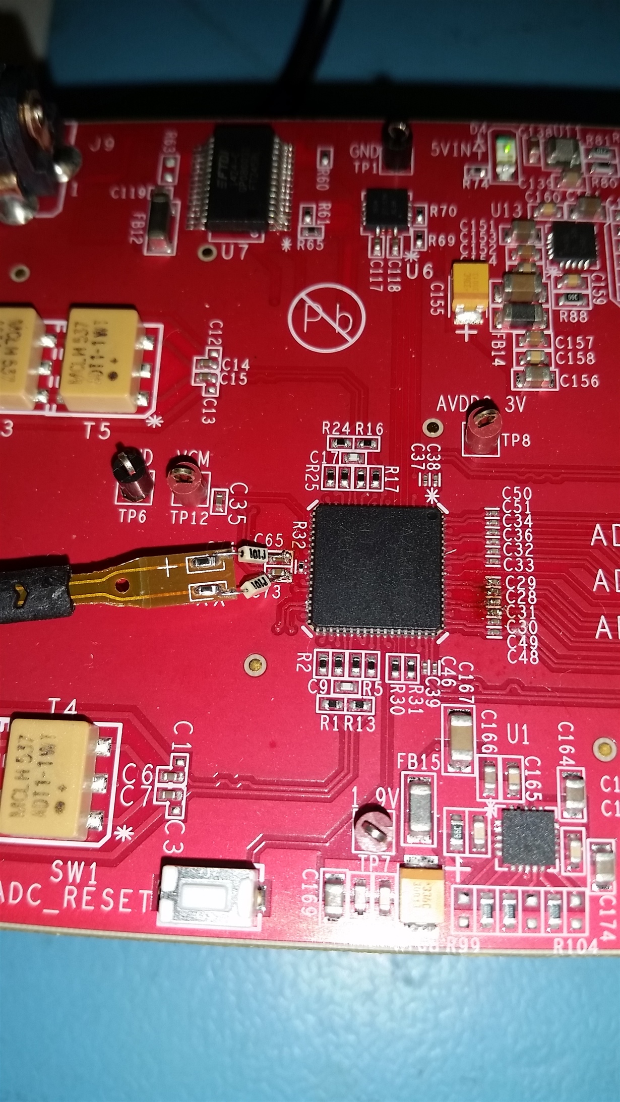
    Yesterday evening I soldered a 16 GHz high impedance probe to the termination resistor R32 (the solder point is on the capacitors C65 and C73 which connect to R32) as shown on the attached photo. Configuration of the LMK is attached.

    Then I simply move the analog delay from 700 ps, 800 ps, 900 ps and finally at 950 ps... no clock!

    Here the screen shots from by scope LeCroy SDA760Zi-A:

    Please tell me I do something wrong which is very simple and stupidly easy to solve! I simply do not get what this is:

    Cheers

    Goran

    Analog delay of 700 ps:

    Analog delay of 800 ps:

    Analog delay of 900 ps:

    Analog delay of 950 ps:

    MG84_LMK04828_250MHz_3MHz90625_1000MHz_700ps_3MHz90625.zip

  • Jim,

    I updated my log "Dec 5, 2018 3:13 PM" with the config files... looks like the attachment only looks odd when editing, but later on the webpage is is correctly inserted as files.

    Cheers
    Goran
  • Goran,

    This sounds like an issue with the LMK device. Our group does not support this part. Can you send this post to the Clock and Timing forum? I will check with the contacts I have as well regarding this.

    Regards,

    Jim 

  • Hello Jim,

    I understand.... But before you had this case over to your colleagues: Could you try to shift the analog delay below 95p ps with your Altera/Intel board... then at least I have accomplished this task.

    Cheers

    Goran

  • Hello Jim,

    We found the problem. A colleague switched by fortune the "ADLY Input" to "Divider + DCC" instead of the "Divider" setting and immediately everything was fine, the clock is now clean and strong, my phase shifting working over the whole range as expected by noble theory.
    The bit which was set is the "DCLKoutX_ADLY_MUX". Unfortunately the datasheet is not very explicit, it tells something about duty cycle correction... on page 57 TI states "This register selects the input to the analog delay for the device clock. Used when DCLKoutX_MUX = 3." on the other hand on page 35 in the diagram it looks like DCC it's a stage after the ADLY. No idea why and how such a duty cycle correction would affect the output signal when I drive the analog delay.
    Whatever, I have now a working setup for some unknown reason.

    Cheers
    Goran