This thread has been locked.

If you have a related question, please click the "Ask a related question" button in the top right corner. The newly created question will be automatically linked to this question.

ADS1247 SPI

Other Parts Discussed in Thread: ADS1247

Hello, I'm having trouble to communicate with the ADS1247.
I'm trying to read the registers but is not working.

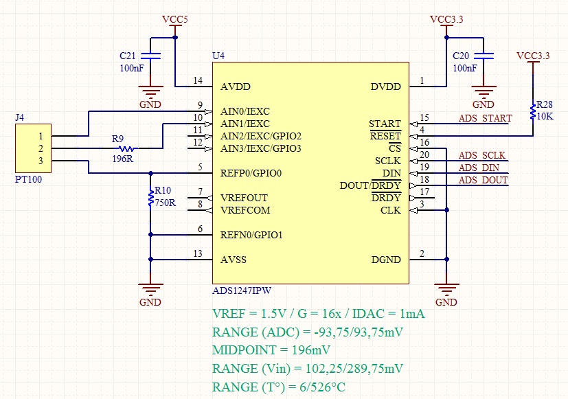
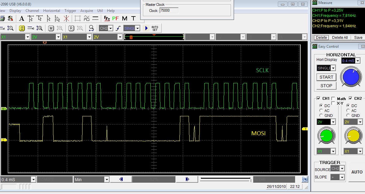
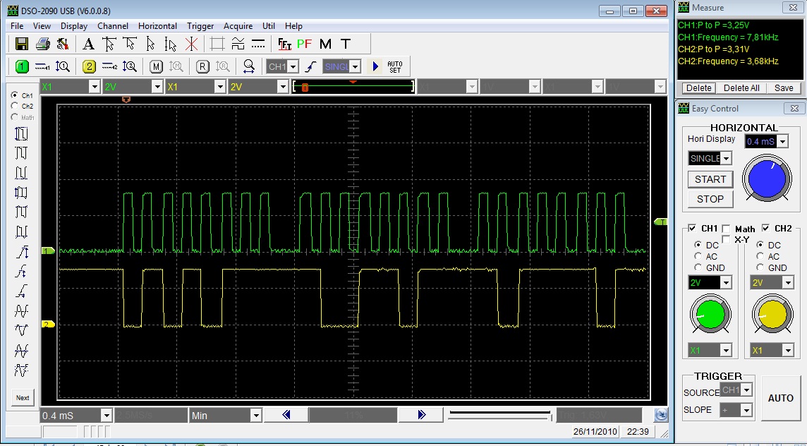
I'm managing only lines SCK, MISO and MOSI, line START I always leave on a high level and line level in CS always let down.

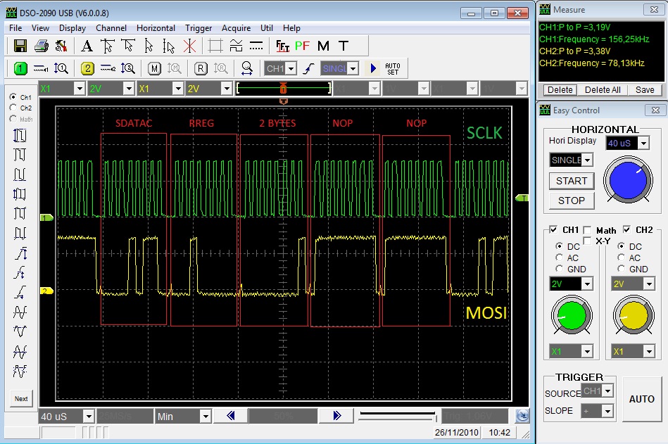
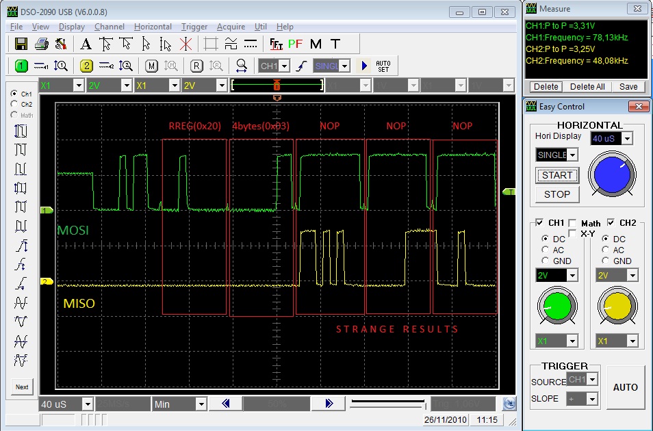
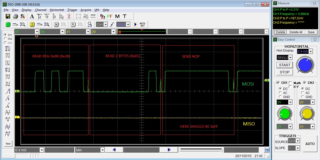
With the oscilloscope looked at the waveforms, and signals CLK and MOSI seem to agree, but I'm not getting the ADS1247 useful information.

I am using ARM LPC1343, and the following code in C:

i2c_buff [0] = 0x20;
i2c_buff [1] = 0x03;
i2c_buff [2] = 0xFF;
i2c_buff [3] = 0xFF;
i2c_buff [4] = 0xFF;
i2c_buff [5] = 0xFF;
lpc1xxx_ssp_send (i2c_buff, 6);
lpc1xxx_ssp_receive (i2c_buff, 4);

I load the data into a buffer and sent to the function ssp.

void lpc1xxx_ssp_send (volatile unsigned char * p, unsigned int bytes)
{
unsigned int i;
for (i = 0; i <bytes; i + +)
{
/ / Only load if not busy and the TX FIFO is not full
while ((LPC_SSP-> SR & (0x02 | 0x10))! = 0x02);
LPC_SSP-> DR = * p;
p + +;
}
}

void lpc1xxx_ssp_receive (volatile unsigned char * p, unsigned int bytes)
{
unsigned int i;
for (i = 0; i <bytes; i + +)
{
/ / Wait while the RX FIFO is empty
while (! (LPC_SSP-> SR & 0x04));
* P = LPC_SSP-> DR;
p + +;
}
}

  • Hi styg,

    Could you perhaps include the schematic around your ADS1247 and maybe screen shots of your SPI interface?  The code snippet seems fine.

  • Styg,

    Review Table26 on page 49 of the datasheet.  You must write commands that tell the ADS1247 which operations you want to perform.  You need to make sure your array values are correct.  For example, your write command is incorrect.  A write starts with a 0x4x followed by the byte representation with the number of bytes to write-1.  The x value in the first byte refers to the register you want to start with.  So 0x40 0x00 0x21 would write to register '0' one byte with the value of 0x21.  The read works in a similar way except the first byte is 0x2x.

    One further thing to note, with the Start pin high the ADS1247 is in read data continuously (RDATAC) mode unless you command it to stop using SDATAC command.  When reading and writing register values you should always SDATAC before the register operations take place.  When you have completed the register operations you can then return to RDATAC mode.  The reason you want to do this is to make sure that your communication does not get corrupted if you happen to be doing a data transfer the same time the conversion result gets placed into the data output register.

    Best regards,

    Bob B

  • It is true the word to write in the reg was wrong, now remade the code taking into account their suggestions.

    i2c_buff [0] = 0x16 / / SDATAC
    lpc1xxx_delay_ms (1);
    i2c_buff [0] = 0x20 / / Streams
    i2c_buff [1] = 0x03;
    i2c_buff [2] = 0xFF;
    i2c_buff [3] = 0xFF;
    i2c_buff [4] = 0xFF;
    i2c_buff [5] = 0xFF;
    lpc1xxx_ssp_send (i2c_buff, 6);
    lpc1xxx_ssp_receive (i2c_buff, 4);

    It seems that things have improved a little, but I'm not sure yet reading.
    I am testing only reading, and it is giving problem. After running the above code, my buffer contains the values:

    i2c_buff = {0x00, 0x01, 0x00, 0x20}

    But according to the datasheet should be:

    i2c_buff = {0x01, 0x00, 0x00, 0x00}

    A doubt, the values of these registers return to default value to each reset, correct?

  • bytes sended by lpc1343

  • These waveforms are the MOSI and MISO lines, making the reading of four REGs after RESET (without writing the REGs), and disabling DATACAR.
    My oscilloscope only has two channels so it's pretty limited.
    Code:


    unsigned char ssp_buff[8];
    ssp_buff[0] = 0x16;        // SDATAC
    lpc1xxx_delay_ms(1);
    lpc1xxx_ssp_send(ssp_buff,1);
    ssp_buff[0] = 0x20;        // RREG
    ssp_buff[1] = 0x03;
    ssp_buff[2] = 0xFF;   
    ssp_buff[3] = 0xFF;   
    ssp_buff[4] = 0xFF;   
    ssp_buff[5] = 0xFF;   
    lpc1xxx_ssp_send(ssp_buff,6);
    lpc1xxx_ssp_receive(ssp_buff,4);   

  • Styg,

    Thanks for all the pictures.  As per datasheet  page 51, "The SDATAC command takes effect after the next DRDY."  I think what you are seeing is data in the output register.  Try a delay between the SDATAC command and the read register command to make sure that the SDATAC command has been activated.

    Best regards,

    Bob B

  • Yeah, actually I had done that but still does not work (delay 1ms).

    It seems that my problem is similar to the other post I saw here in the forum, because usually what I'm getting the ADS is 0x00.

    I have some questions:

    1) The NOP command must be sent only when reading from a register or data, right? NOP does not need to send another time.

    2) The START line, if high level sends data continuously, but at a low level, goes into sleep? What to do with it?

    3) The CS line, I need to keep changing? Or I can leave at a low level?

    4) How should be set CPOL and CPHA bits of the SPI bus?

    5) What is the maximum frequency of the CLK?

  • Styg,

    A 1ms delay is not long enough.  Default data rate is 5sps, so you need at least 200ms before the SDATAC is completed.

    1) A NOP command is needed as the SPI is full duplex, so any time you are actually getting data you should send the NOP.

    2) When the START pin is low, the analog portion of the part is asleep.  You will need to pull the START pin high if you want the device to start converting.  The digital portion is still active when the analog portion is asleep. 

    3) You can leave CS low if this is the only device in your system that is SPI.

    4&5) See the timing diagram Figure 1 on page 10 of the datasheet.  Maximum SCLK frequency is minimum period of 500ns (2MHZ).  SCLK idles low, data is shifted into DIN on the falling edge of SCLK and shifted out of DOUN on the falling edge of SCLK.

    Best regards,

    Bob B

  • Now I noticed that the time that I have to wait after sending the command SDATAC has to be greater than 200ms (because the default sample rate is 5SPS), so now I'm using 300ms of delay.

    CPHA and CPOL am using = 0.

    Waveforms attempt to read the reg IDAC1 (Default 0xFF).

  • Styg,

    The problem with two channel scopes is that you can't see everything at once.  Can you resubmit a plot of the SCLK and MOSI just so we can verify the timing?

    Thanks,

    Bob B

  • Styg,

    Notice that the edges have shifted from what you had previously.  The ADS124x reads the data on the falling edge, so you should see a solid high at the third clock high to low transition for example.

    Best regards,

    Bob B

  • Hi Bob, I did not understand what you mean. After setting my CPHA is right? I'm using CPHA = 0.

    I continued testing here, and I'm able to read anything, although it seems unstable environment.
    Using the code below, I managed to set the regs and make a diode reading.

    ssp_buff [0] = 0x16 / / SDATAC
    lpc1xxx_ssp_send (ssp_buff, 1);
    lpc1xxx_delay_ms (300);
    ssp_buff [0] = 0x42 / / WREG
    ssp_buff [1] = 0x01;
    ssp_buff [2] = 0x23;
    ssp_buff [3] = 0x41;
    lpc1xxx_ssp_send (ssp_buff, 4);
    ssp_buff [0] = 0x22 / / Streams
    ssp_buff [1] = 0x01;
    ssp_buff [2] = 0xFF;
    ssp_buff [3] = 0xFF;
    lpc1xxx_ssp_send (ssp_buff, 4);
    lpc1xxx_ssp_receive (ssp_buff, 2);
    i2c_buff [0] = 0x12 / / RDATA
    lpc1xxx_ssp_send (i2c_buff, 1);
    lpc1xxx_delay_ms (300);
    i2c_buff [0] = 0xFF;
    i2c_buff [1] = 0xFF;
    i2c_buff [2] = 0xFF;
    lpc1xxx_ssp_send (i2c_buff, 3);
    lpc1xxx_ssp_receive (i2c_buff, 3);

    The value of diode read:


    Looking at the waveforms, the value seems to be 0x579BBD. How do I calculate the temperature from that?


    So I need to know if the configuration of the CPHA is right, because it seems it's working but I'll try some more tomorrow.

  • Styg,

    I had to look it up as I don't recall off the top of my head what transitions when CPOL is high or low.  Same is true for CPHA.  I always refer to the actual timing diagram for the device to make sure I'm transitioning properly.

    CPOL=0

    CPHA=1

    Use these values and then verify that it matches the device timing diagram.

    Best regards,

    Bob B

  • Hello Bob, I'm testing with CPOL = 0 and CPHA = 1, it is apparently working.

    As for the diode temperature reading (I'm doing to test), I'm configuring with MUX1 REG 0x33, correct?

    I did a reading and got the value 0x6667FF, could you help me with the calculated temperature from this value?

  • Styg,

    The 0x33 is correct, but your data output is way wrong.  The number you are reading is near full scale, and it should be reading out a converted value of 118mV.  You may want to read back your register to verify that it is showing 0x33 for MUX1.

    Also, you did restart conversions right?

    Best regards,

    Bob B

  • Man, this is strange, I write and I read in REGs REGs of the right values.

    Following is the code I'm using:

    / / Send command SDATAC (0x16) to access the regs without interruption and waits
    / / Sufficient time to occur and command the next DRDY SDATAC take effect
    i2c_buff [0] = 0x16;
    lpc1xxx_ssp_send (i2c_buff, 1);
    lpc1xxx_delay_ms (500);
    / / Send command WREG (0x40) to write the first 4 control regs
    i2c_buff [0] = 0x40;
    i2c_buff [1] = 0x03;
    i2c_buff [2] = 0x01 / / MUX0 (current off burnout, in = AIN0, in-AIN1 =)
    i2c_buff [3] = 0x00 / / Vbias (no bias voltage applied)
    i2c_buff [4] = 0x33 / / MUX1 (int osc.. ref. int. on, ref0, normal)
    i2c_buff [5] = 0x41 / / sys0 (16x gain, 10SPS)
    lpc1xxx_ssp_send (i2c_buff, 6);
    lpc1xxx_ssp_receive (i2c_buff, 3);
    / / Send command WREG (0x40) to write the regs and IDAC0 IDAC1
    i2c_buff [0] = 0x4A;
    i2c_buff [1] = 0x01;
    i2c_buff [2] = 0x0E, / / IDAC0 (DRDY and DOUT on the same pin, I = 1mA)
    i2c_buff [3] = 0x01 / / IDAC1 (current at the entrances and AIN0 AIN1)
    lpc1xxx_ssp_send (i2c_buff, 4);
    i2c_buff [0] = 0x20 / / Streams
    i2c_buff [1] = 0x03;
    i2c_buff [2] = 0xFF;
    i2c_buff [3] = 0xFF;
    i2c_buff [4] = 0xFF;
    i2c_buff [5] = 0xFF;
    lpc1xxx_ssp_send (i2c_buff, 6);
    lpc1xxx_ssp_receive (i2c_buff, 4);
    i2c_buff [0] = 0x2A, / / Streams
    i2c_buff [1] = 0x01;
    i2c_buff [2] = 0xFF;
    i2c_buff [3] = 0xFF;
    lpc1xxx_ssp_send (i2c_buff, 4);
    lpc1xxx_ssp_receive (i2c_buff, 2);


    dl600_read_ads1247 unsigned int (void)
    {
    unsigned int reading;
    i2c_buff [0] = 0x12;
    lpc1xxx_ssp_send (i2c_buff, 1);
    lpc1xxx_delay_ms (500);
    i2c_buff [0] = 0xFF;
    i2c_buff [1] = 0xFF;
    i2c_buff [2] = 0xFF;
    lpc1xxx_ssp_send (i2c_buff, 3);
    lpc1xxx_ssp_receive (i2c_buff, 3);
    read = i2c_buff [0] <<16 i2c_buff [1] <<8 i2c_buff [2];
    return reading;
    }

  • Styg,

    So in the function dl600_read_ads1247 unsigned int (void), the variable is 'reading' that is returned, but the value is saved to 'read'.  I don't think that operation is correct anyway as I believe that those values need to be summed.

    Also, you never restart conversions (0x14 or 0x15) so who knows what will be in the data output register.  If you want to just make one conversion do RDATAC then  you can do SLEEP, WAKEUP and SLEEP commands.  When DRDY goes low you should have a valid reading.  In this case you do not need give the RDATA command.  When DRDY goes low, the first SCLK starts outputting the contents of the data output register.

    Best regards,

    Bob B

  • Look, it is really difficult to talk to this ADS1247!
    Now I'm controlling / verifying also the lines DRDY, and START

    Now I did a test to see if I really am writing in REGs, writing in the reg to change the sampling rate.

    The configuration I do is this:

    LPC_GPIO2-> DATA | = (1 <<ADS_START) / / START HIGH
    i2c_buff [0] = 0x16;
    lpc1xxx_ssp_send (i2c_buff, 1); / / SEND SDATAC
    lpc1xxx_delay_ms (500) / / WAIT FOR DRDY
    / / Send command WREG (0x40) to write the first 4 control regs
    i2c_buff [0] = 0x40;
    i2c_buff [1] = 0x03;
    i2c_buff [2] = 0x01 / / MUX0 (current off burnout, in = AIN0, in-AIN1 =)
    i2c_buff [3] = 0x00 / / Vbias (no bias voltage applied)
    i2c_buff [4] = 0x33 / / MUX1 (int osc.. ref. int. on, ref0, diode)
    i2c_buff [5] = 0x4F, / / sys0 (16x gain, 2000SPS)
    lpc1xxx_ssp_send (i2c_buff, 6);
    / / Send command WREG (0x40) to write the regs and IDAC0 IDAC1
    i2c_buff [0] = 0x4A;
    i2c_buff [1] = 0x01;
    i2c_buff [2] = 0x06 / / IDAC0 (DRDY and DOUT separated, I = 1mA)
    i2c_buff [3] = 0x01 / / IDAC1 (current at the entrances and AIN0 AIN1)
    lpc1xxx_ssp_send (i2c_buff, 4);
    LPC_GPIO2-> DATA & = ~ (1 <<ADS_START) / / START LOW

    With this startup, I can see on the oscilloscope sampling rate actually moved to 2000sps (picture)

    To read it, I use this code:

    unsigned int reading;
    LPC_GPIO2-> DATA | = (1 <<ADS_START) / / START HIGH
    lpc1xxx_delay_us (1);
    LPC_GPIO2-> DATA & = ~ (1 <<ADS_START) / / START LOW
    while (! ADS_DRDY);
    while (ADS_DRDY);
    i2c_buff [0] = 0xFF;
    i2c_buff [1] = 0xFF;
    i2c_buff [2] = 0xFF;
    lpc1xxx_ssp_send (i2c_buff, 3);
    lpc1xxx_ssp_receive (i2c_buff, 3);
    read = i2c_buff [0] <<16 + i2c_buff [1] <<8 + i2c_buff [2];
    return read;


    But I still can not read consistent values for the internal temperature sensor.

    And a question, why the DRDY signal (picture) looks like it was inverted?


  • Styg,

    If there isn't a challenge where would the fun be?  Or sense of accomplishment?

    One thing that I neglected to tell you in the last post is the output code is binary two's complement.  That means that 'read' (which is still defined as 'reading' in your code and you need to fix it) should be a signed value.  You will need to sign extend the 24 bit value to 32bit (?) so that the sign shows the proper value for the code represented.

    I'm a little confused as to how your code works for read/write.  If you send the RDATA command the next 24 SCLKS will output the data, but it appears that you send 24 clocks of writing data first.  Then send another 24 SCLKS to read.  I think you will need to adapt your code so that the reading of registers is correct, or in this case the reading of the conversion data.

    You also asked about the waveform.  This is what it looks like if the data is not read.  DRDY goes high after the first SCLK. 

    Best regards,

    Bob B

  • I need to clarify some points:

    1) When in sleep mode, only the portion of the spi stops working? He continues to do conversions?

    2) When I give a high pulse on the START, and I await the time of conversion (DRDY low level) I still need to send the byte RDATA or only the 3-byte NOP Reading?

    3) After reading a REG I need to send a NOP for DRDY to go to high level?

    4) The registrar OFC and FSC, are restored to each RESET right?

    5) When the ADS is initialized, it is in continuous mode, even if I send the command SDATAC, the final result is in the SPI bus is not it? So when I send other commands (for example to set the REGs) he will not put on the DOUT this result? I ask this because I'm noticing that when I read a REG, before sending the NOP command to return the value, ie when sending the command itself (eg 0x20), I already see some data on the MISO line

  • styg said:

    I need to clarify some points:

    1) When in sleep mode, only the portion of the spi stops working? He continues to do conversions?

        BB> There are two ways to place the part in sleep mode.  One is with the START pin (going low) and the other is with the SPI command.  When placing the part in SLEEP, the conversion in process completes before going to SLEEP.  You can use RDATA command to read the data.  One thing to consider.  When using the SPI SLEEP command you must keep CS low the entire time you want the device to stay in SLEEP.  If you raise CS high at any time, the device goes to WAKE automatically.  This does not happen if you use the START pin for sleep.  The part will remain in SLEEP mode until you pull the pin high.   In either case, when the device is in SLEEP condition the SPI will continue to function, but the only commands that work are RDATA, RDATAC, SDATAC, WAKEUP and NOP (page37 of the datasheet.)

    2) When I give a high pulse on the START, and I await the time of conversion (DRDY low level) I still need to send the byte RDATA or only the 3-byte NOP Reading?

        BB> You need only send 24 SCLKs (with NOP for DIN) to read out the data the first time.  Once DRDY goes back high, you will need to use the RDATA command if you want to read the data a second (or subsequent) time.

    3) After reading a REG I need to send a NOP for DRDY to go to high level?

        BB> If DRDY is low, that means there is conversion data to be read from the ouptut register (3 bytes).  After the first SCLK, DRDY will go high.  As the SPI is full duplex, you always need to send NOP when reading from any of the registers.  Obviously, if you are sending a command and command specific data, that is actual values.  At any other time DIN should be receiving NOP.  You can send a command at the reading of the third byte of conversion data.  I know that sounds a bit confusing, but basically if DRDY is low, then the conversion result is in the data output register and will start clocking out as soon as a SCLK is detected.

    4) The registrar OFC and FSC, are restored to each RESET right?

        BB> When you power up, or RESET the device, the values in the OCR and FSC are set to the factory reset values.

    5) When the ADS is initialized, it is in continuous mode, even if I send the command SDATAC, the final result is in the SPI bus is not it? So when I send other commands (for example to set the REGs) he will not put on the DOUT this result? I ask this because I'm noticing that when I read a REG, before sending the NOP command to return the value, ie when sending the command itself (eg 0x20), I already see some data on the MISO line

        BB> As per page 51 of the datasheet, SDATAC takes effect after the next DRDY.  Before writing or reading of registers you will need to clear out the data in the output register.  So, you send the SDATAC command.  If DRDY is low when the command is sent, you will need to send enough clocks to read out all 24 bits, and do it again if DRDY returns low (that is read the output data).  If DRDY is high when you send the SDATAC command, you will need to wait for DRDY to go low and then read out the 24 bits of data.  Once the result data is cleared from the output register, you can safely read and write the other registers.

  • Forgot to put in the datasheet VREFCOM have to be connected to earth, so that the internal reference works!

    Now I'm able to read some values of the internal temperature sensor, but is very varied, the saga continues.

  • Styg,

    Yes, VREFCOM should be connected to ground, and you must also have a capacitor between VREFOUT and VREFCOM.  Please review page 29 of the datasheet where it discusses this within the section titled Internal Voltage Reference.

    Best regards

  • Thanks Bob, really that's what was missing, with the capacitor, the variation in reading the internal temperature decreased significantly.

    I am still having problems as to stability, because not always does he boots it reads correctly, looks like he's crazy.

    I bought a logic analyzer especially to deal with this guy, but might take a while to arrive, he'll be able to investigate what is happening and I will post here.