This thread has been locked.

If you have a related question, please click the "Ask a related question" button in the top right corner. The newly created question will be automatically linked to this question.

DAC38RF80EVM: Programming and Configuration settings

Part Number: DAC38RF80EVM
Other Parts Discussed in Thread: LMK04828, DAC38RF80

Hello,

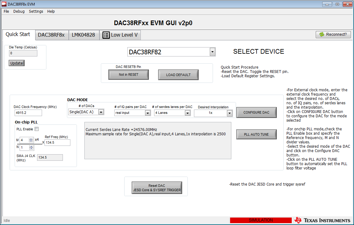
When configuring the DAC38RF80EVM (such as interpolation rate, clock frequency, etc.), do the settings remain on the board when power is cycled or will it have to be reprogrammed each time? There is no easy way to tell with the GUI as you can't read and upload current configuration parameters into the program (a possible software improvement for a future revision)

And to verify, the board's configuration settings can be programmed through the FMC connector using the JESD204 standard correct?

Thanks, 

Jared

  • Hi Jared
    The DAC38RF90EVM does not retain the device settings when it is powered down. It needs to be configured each time it is turned on.
    The default EVM configuration requires device programming to occur using the on-board USB interface and the DAC38RF8xEVM GUI software. (www.ti.com/.../slac722).
    The board can be reconfigured (resistors must be removed and others added) to enable configuration of the DAC38RF80 and LMK04828 devices over the FMC interface. The JESD204 standard does not include FMC based configuration of on-board devices. That configuration signaling must be added into the firmware/software in the carrier card that the DAC38RF80EVM is connected to.
    I hope this is helpful.
    Best regards,
    Jim B
  • Jim,

    Would there be any tutorials or guidance given on how to accomplish configuration through an FPGA  by the method you outlined above? Like which specific resistors to remove and/or add and the signaling required to be sent to the carrier card in order to adjust the firmware per the desired configuration settings?

    Thanks for your help thus far and any future insight,

    Jared

  • Hi Jared

    We don't have an integrated document describing everything that is necessary.

    You can identify which resistors you need to remove/add by reviewing the DAC38RF80EVM design documents which can be downloaded at the link below. The LMK related resistors are on sheet 7 while the DAC related resistors are on sheet 2.

    Please note the signaling level for the LMK04828 device is 3.3V logic while the DAC uses 1.8V logic. You may need extra circuitry on your carrier card to ensure the logic levels are correct.

    There are two issues regarding device configuration programming. 

    1) How to program the devices:

    The DAC and LMK devices will need a specific signaling pattern to properly transfer the address and data information.

    You may use the attached "DAC38RF8x.txt" file to determine the patterns needed for the SPI transaction. It may be best viewed in Excel spreadsheet.

    Write																																																			
    0	0	0	1	0	1	0	1	0	1	0	1	0	1	0	1	0	1	0	1	0	1	0	1	0	1	0	1	0	1	0	1	0	1	0	1	0	1	0	1	0	1	0	1	0	1	0	1	0	1	0	0	0	0	1	0	1	0	1	0	1	0	1	0	1	0	1	0	1	0	1	0	1	0	1	0	1	0	1	0	1	0	1	0	1	0	1	0	1	0	1	0	1	0	1	0	1	0	1	0	1	0	0
    1	0	0	0	0	0	0	0	0	0	1	1	0	0	0	0	1	1	0	0	0	0	0	0	0	0	0	0	0	0	0	0	0	0	0	0	0	0	0	0	0	0	0	0	A10	A10	A9	A9	A8	A8	A7	A7	0	0	0	A6	A6	A5	A5	A4	A4	A3	A3	A2	A2	A1	A1	A0	A0	D15	D15	D14	D14	D13	D13	D12	D12	D11	D11	D10	D10	D9	D9	D8	D8	D7	D7	D6	D6	D5	D5	D4	D4	D3	D3	D2	D2	D1	D1	D0	D0	0	0
    2	0	0	0	0	0	0	0	0	0	0	0	0	0	0	0	0	0	0	0	0	0	0	0	0	0	0	0	0	0	0	0	0	0	0	0	0	0	0	0	0	0	0	0	0	0	0	0	0	0	0	0	0	0	0	0	0	0	0	0	0	0	0	0	0	0	0	0	0	0	0	0	0	0	0	0	0	0	0	0	0	0	0	0	0	0	0	0	0	0	0	0	0	0	0	0	0	0	0	0	0	0	0
    3	1	0	0	0	0	0	0	0	0	0	0	0	0	0	0	0	0	0	0	0	0	0	0	0	0	0	0	0	0	0	0	0	0	0	0	0	0	0	0	0	0	0	0	0	0	0	0	0	0	0	1	1	0	0	0	0	0	0	0	0	0	0	0	0	0	0	0	0	0	0	0	0	0	0	0	0	0	0	0	0	0	0	0	0	0	0	0	0	0	0	0	0	0	0	0	0	0	0	0	0	0	1
    4	0	0	0	0	0	0	0	0	0	0	0	0	0	0	0	0	0	0	0	0	0	0	0	0	0	0	0	0	0	0	0	0	0	0	0	0	0	0	0	0	0	0	0	0	0	0	0	0	0	0	0	0	0	0	0	0	0	0	0	0	0	0	0	0	0	0	0	0	0	0	0	0	0	0	0	0	0	0	0	0	0	0	0	0	0	0	0	0	0	0	0	0	0	0	0	0	0	0	0	0	0	0
    5	0	0	0	0	0	0	0	0	0	0	0	0	0	0	0	0	0	0	0	0	0	0	0	0	0	0	0	0	0	0	0	0	0	0	0	0	0	0	0	0	0	0	0	0	0	0	0	0	0	0	0	0	0	0	0	0	0	0	0	0	0	0	0	0	0	0	0	0	0	0	0	0	0	0	0	0	0	0	0	0	0	0	0	0	0	0	0	0	0	0	0	0	0	0	0	0	0	0	0	0	0	0
    6	0	0	0	0	0	0	0	0	0	0	0	0	0	0	0	0	0	0	0	0	0	0	0	0	0	0	0	0	0	0	0	0	0	0	0	0	0	0	0	0	0	0	0	0	0	0	0	0	0	0	0	0	0	0	0	0	0	0	0	0	0	0	0	0	0	0	0	0	0	0	0	0	0	0	0	0	0	0	0	0	0	0	0	0	0	0	0	0	0	0	0	0	0	0	0	0	0	0	0	0	0	0
    7	1	1	1	1	1	1	1	1	1	1	1	1	1	1	1	1	1	1	1	1	1	1	1	1	1	1	1	1	1	1	1	1	1	1	1	1	1	1	1	1	1	1	1	1	1	1	1	1	1	1	1	1	1	1	1	1	1	1	1	1	1	1	1	1	1	1	1	1	1	1	1	1	1	1	1	1	1	1	1	1	1	1	1	1	1	1	1	1	1	1	1	1	1	1	1	1	1	1	1	1	1	1
    																																																			
    Read																																																			
    0	0	0	1	0	1	0	1	0	1	0	1	0	1	0	1	0	1	0	1	0	1	0	1	0	1	0	1	0	1	0	1	0	1	0	1	0	1	0	1	0	1	0	1	0	1	0	1	0	1	0	0	0	0	1	0	1	0	1	0	1	0	1	0	1	0	1	0	1	0	1	0	1	0	1	0	1	0	1	0	1	0	1	0	1	0	1	0	1	0	1	0	1	0	1	0	1	0	1	0	1	0	0
    1	0	0	0	0	0	0	0	0	0	1	1	0	0	0	0	1	1	0	0	0	0	0	0	0	0	0	0	0	0	0	0	0	0	0	0	0	0	0	0	0	0	0	0	A10	A10	A9	A9	A8	A8	A7	A7	0	1	1	A6	A6	A5	A5	A4	A4	A3	A3	A2	A2	A1	A1	A0	A0	0	0	0	0	0	0	0	0	0	0	0	0	0	0	0	0	0	0	0	0	0	0	0	0	0	0	0	0	0	0	0	0	0	0
    2	0	0	0	0	0	0	0	0	0	0	0	0	0	0	0	0	0	0	0	0	0	0	0	0	0	0	0	0	0	0	0	0	0	0	0	0	0	0	0	0	0	0	0	0	0	0	0	0	0	0	0	0	0	0	0	0	0	0	0	0	0	0	0	0	0	0	0	0	D15	D15	D14	D14	D13	D13	D12	D12	D11	D11	D10	D10	D9	D9	D8	D8	D7	D7	D6	D6	D5	D5	D4	D4	D3	D3	D2	D2	D1	D1	D0	D0	0	0
    3	1	0	0	0	0	0	0	0	0	0	0	0	0	0	0	0	0	0	0	0	0	0	0	0	0	0	0	0	0	0	0	0	0	0	0	0	0	0	0	0	0	0	0	0	0	0	0	0	0	0	1	1	0	0	0	0	0	0	0	0	0	0	0	0	0	0	0	0	0	0	0	0	0	0	0	0	0	0	0	0	0	0	0	0	0	0	0	0	0	0	0	0	0	0	0	0	0	0	0	0	0	1
    4	0	0	0	0	0	0	0	0	0	0	0	0	0	0	0	0	0	0	0	0	0	0	0	0	0	0	0	0	0	0	0	0	0	0	0	0	0	0	0	0	0	0	0	0	0	0	0	0	0	0	0	0	0	0	0	0	0	0	0	0	0	0	0	0	0	0	0	0	0	0	0	0	0	0	0	0	0	0	0	0	0	0	0	0	0	0	0	0	0	0	0	0	0	0	0	0	0	0	0	0	0	0
    5	0	0	0	0	0	0	0	0	0	0	0	0	0	0	0	0	0	0	0	0	0	0	0	0	0	0	0	0	0	0	0	0	0	0	0	0	0	0	0	0	0	0	0	0	0	0	0	0	0	0	0	0	0	0	0	0	0	0	0	0	0	0	0	0	0	0	0	0	0	0	0	0	0	0	0	0	0	0	0	0	0	0	0	0	0	0	0	0	0	0	0	0	0	0	0	0	0	0	0	0	0	0
    6	0	0	0	0	0	0	0	0	0	0	0	0	0	0	0	0	0	0	0	0	0	0	0	0	0	0	0	0	0	0	0	0	0	0	0	0	0	0	0	0	0	0	0	0	0	0	0	0	0	0	0	0	0	0	0	0	0	0	0	0	0	0	0	0	0	0	0	0	0	0	0	0	0	0	0	0	0	0	0	0	0	0	0	0	0	0	0	0	0	0	0	0	0	0	0	0	0	0	0	0	0	0
    7	1	1	1	1	1	1	1	1	1	1	1	1	1	1	1	1	1	1	1	1	1	1	1	1	1	1	1	1	1	1	1	1	1	1	1	1	1	1	1	1	1	1	1	1	1	1	1	1	1	1	1	1	1	1	1	1	1	1	1	1	1	1	1	1	1	1	1	1	1	1	1	1	1	1	1	1	1	1	1	1	1	1	1	1	1	1	1	1	1	1	1	1	1	1	1	1	1	1	1	1	1	1

    The same can be applied to the LMK04828 chip.

    Write																																																			
    0	0	0	0	0	0	0	0	0	0	0	0	0	0	0	0	0	0	0	0	0	0	0	0	0	0	0	0	0	0	0	0	0	0	0	0	0	0	0	0	0	0	0	0	0	0	0	0	0	0	0	0
    1	0	0	0	0	0	0	0	0	0	0	0	0	0	0	0	0	0	0	0	0	0	0	0	0	0	0	0	0	0	0	0	0	0	0	0	0	0	0	0	0	0	0	0	0	0	0	0	0	0	0	0
    2	0	0	0	0	0	0	0	0	0	0	0	0	0	0	0	0	0	0	0	0	0	0	0	0	0	0	0	0	0	0	0	0	0	0	0	0	0	0	0	0	0	0	0	0	0	0	0	0	0	0	0
    3	1	1	1	1	1	1	1	1	1	1	1	1	1	1	1	1	1	1	1	1	1	1	1	1	1	1	1	1	1	1	1	1	1	1	1	1	1	1	1	1	1	1	1	1	1	1	1	1	1	1	1
    4	0	0	1	0	1	0	1	0	1	0	1	0	1	0	1	0	1	0	1	0	1	0	1	0	1	0	1	0	1	0	1	0	1	0	1	0	1	0	1	0	1	0	1	0	1	0	1	0	1	1	0
    5	0	0	0	0	0	0	0	A12	A12	A11	A11	A10	A10	A9	A9	A8	A8	A7	A7	A6	A6	A5	A5	A4	A4	A3	A3	A2	A2	A1	A1	A0	A0	D7	D7	D6	D6	D5	D5	D4	D4	D3	D3	D2	D2	D1	D1	D0	D0	0	0
    6	0	0	0	0	0	0	0	0	0	0	0	0	0	0	0	0	0	0	0	0	0	0	0	0	0	0	0	0	0	0	0	0	0	0	0	0	0	0	0	0	0	0	0	0	0	0	0	0	0	0	0
    7	1	0	0	0	0	0	0	0	0	0	0	0	0	0	0	0	0	0	0	0	0	0	0	0	0	0	0	0	0	0	0	0	0	0	0	0	0	0	0	0	0	0	0	0	0	0	0	0	0	1	1
    																																																			
    Read																																																			
    0	0	0	0	0	0	0	0	0	0	0	0	0	0	0	0	0	0	0	0	0	0	0	0	0	0	0	0	0	0	0	0	0	0	0	0	0	0	0	0	0	0	0	0	0	0	0	0	0	0	0	0
    1	0	0	0	0	0	0	0	0	0	0	0	0	0	0	0	0	0	0	0	0	0	0	0	0	0	0	0	0	0	0	0	0	0	0	0	0	0	0	0	0	0	0	0	0	0	0	0	0	0	0	0
    2	0	0	0	0	0	0	0	0	0	0	0	0	0	0	0	0	0	0	0	0	0	0	0	0	0	0	0	0	0	0	0	0	0	0	0	0	0	0	0	0	0	0	0	0	0	0	0	0	0	0	0
    3	1	1	1	1	1	1	1	1	1	1	1	1	1	1	1	1	1	1	1	1	1	1	1	1	1	1	1	1	1	1	1	1	1	1	1	1	1	1	1	1	1	1	1	1	1	1	1	1	1	1	1
    4	0	0	1	0	1	0	1	0	1	0	1	0	1	0	1	0	1	0	1	0	1	0	1	0	1	0	1	0	1	0	1	0	1	0	1	0	1	0	1	0	1	0	1	0	1	0	1	0	1	1	0
    5	0	1	1	0	0	0	0	A12	A12	A11	A11	A10	A10	A9	A9	A8	A8	A7	A7	A6	A6	A5	A5	A4	A4	A3	A3	A2	A2	A1	A1	A0	A0	0	0	0	0	0	0	0	0	0	0	0	0	0	0	0	0	0	0
    6	0	0	0	0	0	0	0	0	0	0	0	0	0	0	0	0	0	0	0	0	0	0	0	0	0	0	0	0	0	0	0	0	0	D7	D7	D6	D6	D5	D5	D4	D4	D3	D3	D2	D2	D1	D1	D0	D0	0	0
    7	1	0	0	0	0	0	0	0	0	0	0	0	0	0	0	0	0	0	0	0	0	0	0	0	0	0	0	0	0	0	0	0	0	0	0	0	0	0	0	0	0	0	0	0	0	0	0	0	0	1	1

    A special pattern is also used to perform a reset of the DAC38RF8x device:

    Write
    0	0	0	1	0	1	0	1	0	1	0
    1	0	0	0	0	0	0	0	0	0	0
    2	0	D0	D0	D0	D0	D0	D0	D0	D0	0
    3	1	1	1	1	1	1	1	1	1	1
    4	0	0	0	0	0	0	0	0	0	0
    5	1	0	0	0	0	0	0	0	0	1
    6	0	0	0	0	0	0	0	0	0	0
    7	1	1	1	1	1	1	1	1	1	1
    
    Read																																																			
    0	0	0	1	0	1	0	1	0	1	0	1	0	1	0	1	0	1	0	1	0	1	0	1	0	1	0	1	0	1	0	1	0	1	0	1	0	1	0	1	0	1	0	1	0	1	0	1	0	1	0	0
    1	0	1	1	A6	A6	A5	A5	A4	A4	A3	A3	A2	A2	A1	A1	A0	A0	0	0	0	0	0	0	0	0	0	0	0	0	0	0	0	0	0	0	0	0	0	0	0	0	0	0	0	0	0	0	0	0	0	0
    2	0	0	0	0	0	0	0	0	0	0	0	0	0	0	0	0	0	0	0	0	0	0	0	0	0	0	0	0	0	0	0	0	0	0	0	0	0	0	0	0	0	0	0	0	0	0	0	0	0	0	0
    3	1	1	1	1	1	1	1	1	1	1	1	1	1	1	1	1	1	1	1	1	1	1	1	1	1	1	1	1	1	1	1	1	1	1	1	1	1	1	1	1	1	1	1	1	1	1	1	1	1	1	1
    4	1	1	1	1	1	1	1	1	1	1	1	1	1	1	1	1	1	1	1	1	1	1	1	1	1	1	1	1	1	1	1	1	1	1	1	1	1	1	1	1	1	1	1	1	1	1	1	1	1	1	1
    5	0	0	0	0	0	0	0	0	0	0	0	0	0	0	0	0	0	0	0	0	0	0	0	0	0	0	0	0	0	0	0	0	0	0	0	0	0	0	0	0	0	0	0	0	0	0	0	0	0	0	0
    6	0	0	0	0	0	0	0	0	0	0	0	0	0	0	0	0	0	0	0	0	0	0	0	0	0	0	0	0	0	0	0	0	0	0	0	0	0	0	0	0	0	0	0	0	0	0	0	0	0	0	0
    7	1	1	1	1	1	1	1	1	1	1	1	1	1	1	1	1	1	1	1	1	1	1	1	1	1	1	1	1	1	1	1	1	1	1	1	1	1	1	1	1	1	1	1	1	1	1	1	1	1	1	1
    

    The first column indicates the FTDI device AB bus bits. We have been using AB bus for both DAC38RF8x and LMK04828 devices. For instance, the 0 in the first column stands for ABBUS0.

    For the DAC, you will see row 0 is the SCLK pattern. row 1 is the SDIO write process. row 2 is reading back part of the SDIO read process in three wire mode. row 3 is the SDENB process where it is held high at all time and pulled low during SPI transaction. 

    Other details includes:

    ·         “Ax” indicates “bit x of the address to be written” for both the read and write case. The address is always written for both reading and writing.       Example: A5 refers to 5th address bit(starting from A0)

    ·         “Dx” indicates “bit x of the data to be written” for writing and “bit x of the data to be read” in the read case. The data is written for writing and read for reading.

    ·         The address length and data length for each device is extracted from the file based on the largest address bit and largest data bit (i.e. A31 indicates a 32 bit address).

    ·         Except for the pin from where the read bits are received, all other pins are configured to be output pins.

    The LMK device is similarly mapped using rows 4,5,6,7 in that file. The DAC pins are set to static values in the LMK file and vice versa.

    2) What information to program. I recommend using the DAC38RF8x GUI initially to get the EVM up and running in the mode you need. You can see which addresses are being written and read from the Status Log panel. This panel is launched by double clicking on the word Idle in the lower left corner of the main GUI window. Once the Status Log panel is open, you can observe the reads and writes. You can save a copy of this information by clicking in the Status Log window and typing Ctrl-A to select everything, and then right-clicking and choosing Save Selected from the popup.

    I hope this is helpful.

    Best regards,

    Jim B