This thread has been locked.

If you have a related question, please click the "Ask a related question" button in the top right corner. The newly created question will be automatically linked to this question.

Problem with ADS8320 and TLC4541

Other Parts Discussed in Thread: ADS8320, ADS7816, TLC4541

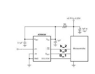
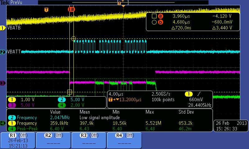
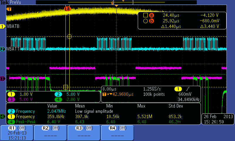
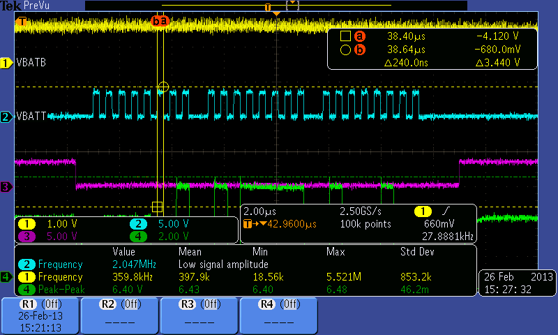
I have a problem with the ADS8320. This it only reads discreet values (for example 32,64,128,256,512,1024,2048, etc.) when it varies my signal of entrance. I try to use a TLC4541 and have the same problem. My comuniacion by SPI works well when proving it with a ADS7816. Some idea?

  • Hi Manuel,

    My first inclination is to suggest you have a clock to data phase relationship issue.  Can you perhaps send us a schematic showing your hookup to the ADC(s) and maybe a screen shot of your SPI interface?

  •  

    thanks for your reply.

    My CIRCUIT is simple. very similar to Figure 8 in the ADS8320 datasheet(
    with a low-pass filter formed with a 47uF capacitor and a resistance of 100 ohm)

    My subrutine in "C" (Within a loop)

    //////////////// Driver for ADS8320 A/D Converter ///////////////////////
    ////                                                                 ////
    ////  init_ext_adc()                      Call after power up        ////
    ////                                                                 ////
    ////  value = read_ext_adc()              Converts to digital number ////
    ////                                      and sends to MCU           ////
    ////                                                                 ////
    /////////////////////////////////////////////////////////////////////////
    ////        (C) Copyright 1996,2003 Custom Computer Services         ////
    //// This source code may only be used by licensed users of the CCS  ////
    //// C compiler.  This source code may only be distributed to other  ////
    //// licensed users of the CCS C compiler.  No other use,            ////
    //// reproduction or distribution is permitted without written       ////
    //// permission.  Derivative programs created using this software    ////
    //// in object code form are not restricted in any way.              ////
    /////////////////////////////////////////////////////////////////////////

    #use delay(clock=16000000)
    #ifndef ADS8320_CS

    #define ADS8320_CLK  PIN_B1
    #define ADS8320_DOUT PIN_B0
    #define ADS8320_CS   PIN_B2

    #endif


    void init_ext_adc() {
       output_high(ADS8320_CS);
       output_high(ADS8320_CLK);
    }


    long read_ext_adc() {
       int i;
       long long data;

       data=0;
       output_low(ADS8320_CS);
       for(i=0;i<=5;i++)             // take sample and send start bit
       {
          output_low(ADS8320_CLK);
          delay_us(1);
          output_high(ADS8320_CLK);
          delay_us(1);
       }
       for(i=0;i<16;++i) {           // send sample over spi
          output_low(ADS8320_CLK);
          delay_us(1);
          shift_left(&data,2,input(ADS8320_DOUT));
          output_high(ADS8320_CLK);
          delay_us(1);
       }

       output_high(ADS8320_CS);
       return(data);
    }

    I appreciate any help

    Thanks


  • Hi Manuel,

    In the ADS8320 datasheet you will see a delay time (tSUCS on page 10) that describes the time from the falling /CS to the first rising SCLK.  Change your code so that the SCLK dwells low while it is inactive.  Next, the sixth SCLK from the falling /CS is a 'null' bit - the device will output a zero while the MSB id being converted, so change your first loop to be   for(i=0;i<=6;i++).  The rest looks OK to me.

  • Thanks for your reply, I make the changes but there was no change

    /////////////// Driver for ADS8320 A/D Converter ///////////////////////
    ////                                                                 ////
    ////  init_ext_adc()                      Call after power up        ////
    ////                                                                 ////
    ////  value = read_ext_adc()              Converts to digital number ////
    ////                                      and sends to MCU           ////
    ////                                                                 ////
    /////////////////////////////////////////////////////////////////////////
    ////        (C) Copyright 1996,2003 Custom Computer Services         ////
    //// This source code may only be used by licensed users of the CCS  ////
    //// C compiler.  This source code may only be distributed to other  ////
    //// licensed users of the CCS C compiler.  No other use,            ////
    //// reproduction or distribution is permitted without written       ////
    //// permission.  Derivative programs created using this software    ////
    //// in object code form are not restricted in any way.              ////
    /////////////////////////////////////////////////////////////////////////

    #use delay(clock=16000000)
    #ifndef ADS8320_CS

    #define ADS8320_CLK  PIN_B1
    #define ADS8320_DOUT PIN_B0
    #define ADS8320_CS   PIN_B2

    #endif


    void init_ext_adc() {
       output_high(ADS8320_CS);
       output_low(ADS8320_CLK);
    }


    long read_ext_adc() {
       int i;
       long long data;

       data=0;
       output_low(ADS8320_CS);
       for(i=0;i<=6;i++)             // take sample and send start bit
       {
          output_high(ADS8320_CLK);
          delay_us(1);
          output_low(ADS8320_CLK);
          delay_us(1);
       }
       for(i=0;i<16;++i) {           // send sample over spi
          output_high(ADS8320_CLK);
          delay_us(1);
          shift_left(&data,2,input(ADS8320_DOUT));
          output_low(ADS8320_CLK);
          delay_us(1);
       }

       output_high(ADS8320_CS);
       return(data);
    }

  • Hi Manuel,

    Please send an oscilloscope shot of the timing (/CS, SCLK, SDO), that will be the easiest way to decipher what's going on.  Please also describe what you do get from the SPI interface - Analog input is X, digital output is Y, etc..  By the code sample above, this should be working.

  • I have seen similar discreet results form my ADS8320HT output. I have made sure that the time between /CS goes low and the first SPI clock is more than 1us. Is there any solution about this issue?

  • Hi Zhengyu,

    A few questions:

    - Are your results repeatable over multiple conversions of a DC input?

    - What reference voltage are you using?

    - Could you please send me an oscilloscope plot showing /CS, DCLK and SDO over 2 or 3 conversion cycles for a given DC input?

    Thanks,

    Harsha

  • - I am sampling a sine signal that generated from a functional generator. It is a 8KHz sine signal and I am sampling at 32Khz. Thus, I am getting 4 ADC value per period

    - I am using a 3v reference voltage.

    - Here are a few screen shot. Yellow is input signal (8KHz sine at 0.426V amplitude and 0.3V offset), Blue is SCLK, pink is /CS, and green is SDO. The ADC's VCC is 5V but I am interface the SPI bus to a processor that with 3.3V VCC. I don't think the 5V as VCC for the ADC should be a concern because I previous use the same 3.3v as VCC for the ADC and it behave the same.

    - the SPI clock is running at 2.048MHz and I am sampling the ADC data using a DMA engine to generate 3 burst of 8 bit SPI clocks.


  • Here is the data file

    0FD8
    3FE8
    57D0
    3FC4
    0FE9
    3FF0
    57D0
    3FD0
    0FC0
    3FF0
    57C8
    3FE0
    0FEC
    3FE8
    57C1
    3FD0
    0FE7
    3FE9
    57D0
    3FD4
    0FF0
    3FE9
    57C0
    3FD0
    0FE0
    3FE1
    57C8
    3FD0
    0FE6
    3FE8
    57C5
    3FD0
    0FF0
    3FF0
    57C4
    3FD0
    0FE6
    3FE8
    57D0
    3FD0
    0FE9
    3FE8
    57E0
    3FD0
    0FF2
    3FF0
    57D0
    3FD0
    0FED
    3FEA
    57D0
    3FC4
    0FE9
    3FE8
    57E0
    3FD0
    0FEA
    3FF0
    57D0
    3FD4
    0FF2
    3FEC
    57D0
    3FD1
    0FF1
    3FC0
    57D0
    3FD0
    0FC0
    3FEA
    57C9
    3FE0
    0FF2
    3FEA
    57D0
    3FD0
    0FF5
    3FF0
    57E0
    3FD0
    0FEA
    3FF0
    57E0
    3FD4
    0FE5
    3FEA
    57CC
    3FD0
    0FEC
    3FEC
    57E0
    3FD0
    0FF0
    3FEB
    57D4
    3FD0
    0FE4
    3FF0
    57D0
    3FE0
    0FE8
    3FE8
    57D0
    3FD1
    0FE1
    3FF0
    57E0
    3FD0
    0FE8
    3FE8
    57C4
    3FD0
    0FE3
    3FF0
    57E0
    3FD0
    0FF2
    3FF0
    57C9
    3FD0
    0FE8
    3FF0
    57C8
    3FD1
    0FF0
    3FEC
    57C0
    3FD0
    

  • Hi Zhenyu,

    From the last plot in your post, the ADC seems to be converting just fine. The output word (green trace) being read out is 0x57D1 or 22481 decimal. With a 3V reference, this translates to a corresponding input voltage of 22481*3V/65536 ~= 1.03V. Now, the signal on the yellow trace is noisy, but we can see that the input is at about 1div * 1V/div = 1V, which is pretty close to what we expect. So the ADC appears to be working as it should.

    I see that you have a long delay between ADC conversions as a result of which you are only able to sample the input 4 times per period, instead of 10 times per period, considering your nearly 85KHz conversion cycle (2.048MHz/24). To this end I would recommend reducing the duty cycle of the /CS signal to <5% if possible so that the /CS high phase is minimized to just 1 or 2 cycles.

    Thanks,
    Harsha

  • Hello there,

             The main reason that we are using a 16bit ADC is to get a more accurate reading data and that is why the previous user and I try to point out that this ADC doesn't return ADC reading accurately as we are expecting. Like you also point out, the input signal is quite noise; thus, I expect the reading from ADC should reflect the noise signal. The last 2-3 bits of reading should be fluctuated in reflecting of noise signal but the reading did not show that. As shown in my data file, most of them it is the 3rd or 4th LSB change value. Effectively, I am getting a 12-13bit ADC accuracy instead of 16 bit that i am hoping for. If this is expected like you mentioned, I think I will need to look for alternative solution.

  • Zhenyu,

    Thank you for the clarification. Sorry I misinterpreted your comments. 

    I sorted the data you provided by code and now I understand what you mean by "discrete" ADC outputs. As you have pointed out, the ADS8320 is a 16-bit ADC and the output data should exhibit much more variation for the amount of noise there is on the input signal. The part seems to be showing significant degradation in DNL, which is reducing the resolution of the ADC.

    The loss of resolution is often due to gross variations in reference voltage during conversion. On SAR converters the input impedance of the reference input is dynamic and it changes during conversion. Ideally, a good reference circuit will ensure that the voltage at the reference pin changes by less than 1LSB while the ADC is converting. It would be helpful if you could send me a scope capture of the voltage at the reference pin over 2 or 3 periods of your input signal, as the ADC is converting. I understand that a few LSBs of variation is too small for most oscilloscopes to resolve but any gross problems should show up. If possible could you also send me your schematic showing your reference circuit?

    Thanks,

    Harsha

  • Hello Harsha,

            You are right about the Vref. After adding a tantalum cap on the Vref to ADC, I can see that the last 2 LSB of reading are now changing everytime, which is what i expected. Thank you for your help.

    zhenyu

  • Zhenyu,

    That is good to hear. Please let us know if you have any other questions.

    Best Regards,

    Harsha