This thread has been locked.

If you have a related question, please click the "Ask a related question" button in the top right corner. The newly created question will be automatically linked to this question.

ADS1204: Influence of the Input Source Impedance

Part Number: ADS1204
Other Parts Discussed in Thread: AMC1305M25

Hello,

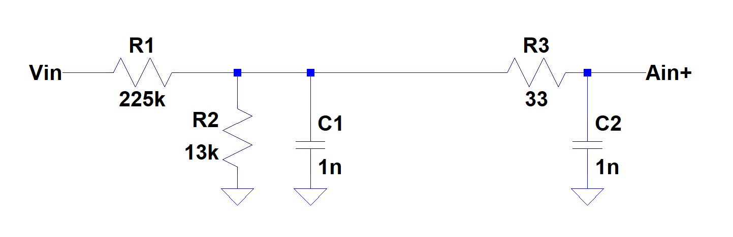
In the data sheet of the ADS1204 the following is mentioned:

"The input impedance (of the ADS1204) becomes a consideration in designs where the source impedance of the input signal is high. This high impedance may cause degradation in gain, linearity and THD.

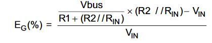
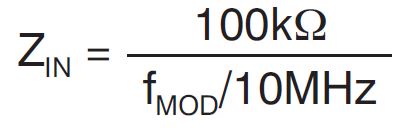
The impedance of my source signal is 12.3kOhm which I will convert into a delta-sigma bitstream using the ADS1204 with an external clock frequency fext of 20MHz. According to the Formula below I calculated an input impedance Zin of 100kOhm (fmod = fext/2). Together they form a voltage divider with a gain of approximately 0.89.

Is there another, additional influence on the gain caused by the high source impedence? What influence does it have on the Linearity and the THD of the output signal? Do you have any recommendations to improve the performance in my specific application?

Thank you!

Best,

Nicole

  • Hi Nicole,

    What sort of sensor are you planning to use with the ADS1204? We generally recommend using a buffer ahead of the inputs (see Figures 26 and 27 in the datasheet) when using a high impedance source.
  • Hi Tom,

    I measure the output voltage of an inverter for a sensorless motor drive application. I have attached a sketch of the input stage, whereas Ain+ is the positive input pin of the ADS1204. It's a single ended measurement and the negative input pin of the ADS1204 (Ain-) is connected to 2.5V. The source signal (Vin) is a sinusoidal signal (fundamental frequency 2kHz, amplitude 90V) which is pulse width modulated (switching frequency 40kHz). The last of the two 1nF is located close to the ADS1204 and is used to buffer the signal. I'd like to know what influence the high source impedance has on the gain, linearity and THD and how the improve the performance by altering the below circuit.

    Thank you and best regards

    Nicole

  • Hi Nicole,

    There is an app note for another one of our modulators that might help here - take a look at TI document number SBAA214.  That app note deals with our AMC1305M25 which has a significantly smaller input voltage range, but the basic principles are the same.  With the ADS1204, you are looking into a switched capacitor and that Zin will be in parallel with your source.  I don't have an easy way to tell you exactly what will happen to the THD, since that will depend to some extent on how you intend to build the digital filter for the modulator output, but you can get an idea of the gain and linearity errors you may see.  You can always calibrate out gain and offset errors, but my suggestion is to insert at least a voltage follower/unity gain buffer between C1 and R3.

  • Hi Nicole,

    Are you able to test your system with and without a buffer on the input to the ADS1204?
  • Hi Tom,

    Thank you for your reply. I've studied the app note SBAA214 dealing with the AMC1305M25. In this document, two methods are suggested to optimize the performance: adding a series resistor at the negative input to eliminate the effect of the bias current or, as a second method, addiging an operational amplifier inbetween the voltage divider and the AMC1305M25. In order to save space and costs I'd prefer the solution with the compensated circuit in order to achieve a good performance. As you mentioned earlier, I can get rid of gain and offset errors by calibration. What I cannot calibrate out is non-linearity.

    Can you provide me with equations suitable to calculate the gain and offset error in my application with the ADS1204 (without the voltage follower) so I can estimate the damage? Is there any compensation circuit available for my application with the ADS1204 similar to the one described in the app note SBAA214? Can you provide me information regarding the linearity of the circuit?

    Thank you and best regards

    Nicole

  • I could try this at a later stage. What changes do you expect? The buffer cap is not so much of an issue to me. The operational amplifier (to be used as a voltage follower) is a much bigger issue regarding costs and space.
  • Hi Nicole,

    The input structures between the ADS1204 and the AMC1305 are a little different. The series 'R' option to compensate for the bias current is not going to be an issue with the ADS1204. You can use the same gain formula, just change the values.
  • Dear Tom,

    Thank you for your message. So basically you are saying, that there is no offset error if we use the ADS1204 with a high source impedance. So in case we don't use a voltage follower, there is only a gain error which can be caluclated with the formula bellow as per the TI document SBAA214. Is that correct?

    Thank you and best regards

    Nicole

  • Hi Nicole,

    Sorry for the confusion here - the AMC1305 device has a VCM block which will cause bias current to flow through your shunt, so the additional series R at the (-) input helps with the offset that causes. I don't have a bias current value for the ADS1204, so there may still be some small offset that you would need to deal with. I also wanted to point out that you are still looking at biasing the (-) input to +2.5V (refer to Figure 26 again), so you should consider buffering that signal at a minimum.