This thread has been locked.

If you have a related question, please click the "Ask a related question" button in the top right corner. The newly created question will be automatically linked to this question.

ADS1256: Setting up the SPI Logic Analyzer for ADS1256

Part Number: ADS1256

Hi Chris,

Sorry for asking too much. I wonder if you could help me with some of the basic logic analyzer setup for the SPI communication debugging on ADS1256?

SCLK - pin 13 (SCK)
DIN - pin 11 (MOSI)
DOUT - pin 12 (MISO)
DRDY - pin 9
CS - pin 10 (CS)
RESET - pin 8 (or tie HIGH?)

For the following pins, which should be set LOW, RISE, HIGH, FALL, or EDGE for the trigger type?

Thanks,

Khoi Ly

  • Hi Khoi,

    It is not a problem at all, we're here to help!

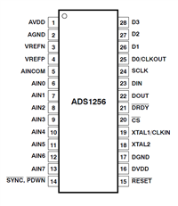
    Unfortunately, I'm sure what pin numbers you're referring to; these are not the same as the ADS1256 pin numbers for the digital signals...

    When communicating with the ADS1256, keep in mind that it uses SPI mode 1 (SCLK is normally low and /DIN and DOUT should be evaluated on the falling edge of SCLK).

    For logic analyzer triggering, it doesn't really matter where you trigger as you as you capture the data you're after. I typically trigger on the falling edge of /CS so that I can see the entire SPI frame.


  • My apology, those pins are not entirely necessary to show to you. They are the pins on Arduino Uno R3.

    I place a digital pin from arduino called DIO7 that triggers right before the microcontroller receiving ADC data from the ADS 1256 (DIO7 Falling edge trigger on the logic analyzer). The CS pin is kept LOW the entire time

    digitalWrite(7,HIGH);

    ....

    digitalWrite(7,LOW);
    adc_val[i] = SPI.transfer(0);
    adc_val[i] <<= 8; //shift to left
    adc_val[i] |= SPI.transfer(0);
    adc_val[i] <<= 8;
    adc_val[i] |= SPI.transfer(0);

    Do you know why the data line (MISO) from this logic analyzer appears to pulse before the clock?

    The first 8 bits are B01111111 ------ The only way that we get a 0 bit in the first spi.transfer is if we begin counting the data line (MISO) before the clock goes HIGH

    The second 8 bits are B11111111 

    The third 8 bits are B10111001 ------ Similarly, the ending bit of the last spi.transfer is 1, but you can see that it is one clock cycle before the last clock pulse

    And we can combine these three 8-bits transmission to obtain a total of 24 bit data.

    drive.google.com/open

  • Hi Khoi,

    Some of our ADC's have a shared DOUT/nDRDY pin, but this device shouldn't have any pulses on DOUT until you send SCLKs...

    Have you by chance looked at the SPI communication on an oscilloscope? Most logic analyzers only show digital LOW/HIGH values, but an oscilloscope can show you analog voltages which might be of use when trying to debug signal integrity (SI) issues. It's possible that the /DRDY signal (or some other nearby signal) could be coupling into your DOUT trace and showing up as a pulse.

    If you are jumper wiring from the Arduino to the ADC, do take care to keep these wires short and make sure you have a nearby ground wire! (I usually wrap the ground wire around other jumper wires to keep the current loop area as small as possible to avoid SI issues).

    Also, what is your input voltage so that I can know what data value you're expecting?
  • I have not tried the scope yet, but based on what you said, I would assume that the scope can handle the sharp corners for digital square waves? In other words, does the scope have enough bandwidth to capture the SPI signal?

    By wrapping the ground wire, I think you mean for each digital signal, I will provide a twisted pair with ground wire?

    I will look into the input voltage as well.

    Maybe what you say about the signal integrity is true, but I wonder why this problem only happens to DOUT (MISO) but not DIN (MOSI)? All of the SPI pins are connected from Arduino to breadboard, then from breadboard they are splitted to the logic analyzer and the ADS1256.

    Thanks,

    Khoi Ly
  • Hi Khoi,

    Depending on the oscilloscope and probe bandwidth, you may not see all of the high frequency effects but I still think it would give more insight into potential SI issues, especially since the logic analyzer tends to hide the effects of noise, overshoot, and ringing. Do make sure to probe as close to the input pins (DIN on the ADC, MISO on the MCU) so that you can view the signal as seen on the receiving end of the trace (probing near the source will not tell you if there are SI issues at the other end of the trace or wire).

    I think one ground wire (around each set of jumper wires) is sufficient, so long as it close to all other signal wires. I usually just wrap a single ground wire around all of my SPI jumper wires, ensuring that it connects the grounds of each board together. Twisted pair wiring on each signal would be more ideal, but I don't think it is necessary in this case. However, since you are jumper wiring from an Arduino to a breadboard, and then from the breadboard to another board, you should probably wrap each set of wires. If you can remove the breadboard and just go between the Arduino and your test-board, I would highly recommend it!


  • Hi Chris,

    I tried your suggestion and I think there is something going on with the oscilloscope results
    drive.google.com/open

    yellow is the clock, it works normally

    Green is the MISO line, it doesn't seem to behave well.

    The timing is consistent with the Logic Analyzer result, so I think maybe I have some problem with the data interpretation rather than the clock pulse timing itself. However I would like to ask the following?

    1. Is it normal for the MISO line remains HIGH at the end of the transmission? The scope shows that there is a gradual decay of the last MISO pulse and this seems wierd to me. The gradual decay cause the system to see the MISO lines remains HIGH after the transmission ends.

    2. The MISO line starts abit above ground then goes abit below ground when pulsing. Is this normal?

    I have someone related questions about ADS 1256:

    1. How do you know the value of SPI Speed? Is it dependent on the microcontroller? What should be a good resource for me to take a look at?

    2.  The following line allows me to setup the status register for the Arduino Uno Microcontroller

    byte status_reg = 0x00 ; // address (datasheet p. 30)
    byte status_data = 0x01; // 01h = 0000 0 0 0 1 => status: Most Significant Bit First, Auto-Calibration Disabled, Analog Input Buffer Disabled
    //byte status_data = 0x07; // 01h = 0000 0 1 1 1 => status: Most Significant Bit First, Auto-Calibration Enabled, Analog Input Buffer Enabled
    SPI.transfer(0x50 | status_reg); // b01010000
    SPI.transfer(0x00); // 2nd command byte, write one register only
    SPI.transfer(status_data); // write the databyte to the register
    delayMicroseconds(100);

    There is a small delay between SPI.transfer in the Arduino that separate the bytes from each other.

    What if my ESP32 sends a stream of 3 bytes back to back with the above SPI.transfer bytes but without any gap between those bytes and the clock will pulse continuously 24 times. Would I have any trouble writing these bytes to the register? 

    https://drive.google.com/file/d/1Bupz8NJ5kKghyv77zVj-VlrwI7yfmwm0/view?usp=sharing

    Thanks,

    Khoi Ly

  • Hi Khoi,

    Unfortunately, I'm not able to access your Google Drive. Would it be possible for you to attach some of the oscilloscope screenshots to your E2E post?...Do make sure to use the "Insert/Edit Media" button as "CTRL-V" pasting doesn't work very well on E2E yet.

    Regarding your questions...

    Khoi Ly10 said:
    1. How do you know the value of SPI Speed? Is it dependent on the microcontroller? What should be a good resource for me to take a look at?

    The SCLK frequency is configurable in most microcontrollers, either by selecting the clock source that the SPI peripheral uses, or by configuring a clock divider. You can try searching for "SPI" or "SPI code examples" for the Arduino. I know of a third-party Github project (here: https://github.com/baettigp/ADS12xx-Library) but I have not tried it.

    The ADS1256 allows for SCLK frequencies as fast as fCLK/2 or 3.84 MHz (for a 7.68 MHz clock).

    Khoi Ly10 said:

    2.  The following line allows me to setup the status register for the Arduino Uno Microcontroller

    byte status_reg = 0x00 ; // address (datasheet p. 30)
    byte status_data = 0x01; // 01h = 0000 0 0 0 1 => status: Most Significant Bit First, Auto-Calibration Disabled, Analog Input Buffer Disabled
    //byte status_data = 0x07; // 01h = 0000 0 1 1 1 => status: Most Significant Bit First, Auto-Calibration Enabled, Analog Input Buffer Enabled
    SPI.transfer(0x50 | status_reg); // b01010000
    SPI.transfer(0x00); // 2nd command byte, write one register only
    SPI.transfer(status_data); // write the databyte to the register
    delayMicroseconds(100);

    There is a small delay between SPI.transfer in the Arduino that separate the bytes from each other.

    What if my ESP32 sends a stream of 3 bytes back to back with the above SPI.transfer bytes but without any gap between those bytes and the clock will pulse continuously 24 times. Would I have any trouble writing these bytes to the register? 

    Certain ADS1256 SPI byte transfers do require a delay (see "t6" in the ADS1256 datasheet). I recommend controlling the /CS with a GPIO (avoid built-in frame sync pins that toggle /CS after each SPI byte) and inserting a delay between SPI.transfer() calls when a delay is necessary.

  • That is okay, I think I figured out the problem with the clock pulse.

    Regarding your replies to my questions, I would like to following the following:

    For question 1. I will keep trying to increase my SPI speed on the microcontroller up to 3.85MHz and see when I begin to lose my communication due to the microcontroller? How do I know if my microcontroller is bottlenecking?

    For question 2. "t6 = Delay from last SCLK edge for DIN to first SCLK rising edge for DOUT." In the case of

    SPI.transfer(0x50 | status_reg); // b01010000
    SPI.transfer(0x00); // 2nd command byte, write one register only
    SPI.transfer(status_data); // write the databyte to the register

    I am sending out signal from micro-controller only, so it should be "Delay from last SCLK edge for DIN to first SCLK rising edge for the next DIN."
    Especially when I am reading 24 bits of data per channel after I use RDATA. In this case it will be "Delay from last SCLK edge for DOUT to first SCLK rising edge for the next DOUT." Can the clock pulse continuously 24 times and I just take the entire chunk of 24 bits?

    Thanks,

    Khoi Ly
  • Hi Khoi,

    1. If you are having signal integrity issues, then it might be a good idea to try using a lower SCLK frequency rather than a higher one. Please note that running SCLK faster than FCLK/2 would be outside of the ADS1256 specifications and is not recommended.
    2. If are in SDATAC mode and use the RDATA command to fetch the data, then you must include the t6 delay after the first command byte (see figure 30 in the ADS1256 datasheet).

      However, if you are in RDATAC mode then you can simply clock out the data by sending 24 continuous clocks, as shown in Figure 32.

    I hope that helps!

  • Hi Chris,

    Thank you for your support. I was able to make the ADS1256 to work with ESP32. However, I encounter the following bug.

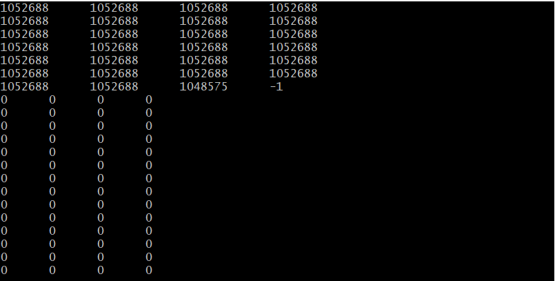
    In differential mode, I measure the voltage of the power supply from 0 to 3V. The program works fine and I am able to log the raw unsigned integer data in the terminal monitor. However, the program breaks occasionally when I increase / decrease the voltage  whose values are in the transition between ~900,000 and ~1,000,000.

    The break behavior is follow: when the data log increases from ~900000 to ~1000,000 the data becomes -1 then 0. After it becomes zero, I can no longer collect data no matter how much I try unless I reset the microcontroller. This behavior is similar when I decreases the value from ~1,000,000 to ~900,000.

    Other than that, the code works fine

    Are you aware of any thing like this? Do you have any suggestions for debugging?

    Thank you,

    Khoi Ly

  • Hi Khoi,

    Do you have a good ground connection between the ADS1256 and the ESP32? This behavior could be explained by a loss of communication, which may result if the MCU and ADC grounds drift apart.

    I'd also recommend comparing this behavior to a logic analyzer capture of the SPI communication to determine if you are indeed losing the communication with the ADC, or if something might be happening in the ESP32 code.


  • I am pretty certain that the issue is not from the losing connecting. Since I only lose the signal whenever I cross the value 900,000 and 1000,000.

    The SPI MOSI indeed gives me flat LOW whenever I lose the data, and I cannot make it work again until I reset the ESP32.

    Thanks,

    Khoi Ly
  • Hi Khoi,

    Do you have an image of your setup that you could share?

  • Here is my setup. I think one of the problem might be the fact that I have to do the following step:

    SPI.transfer(0x01); // Read Data 0000 0001 (01h) // ********** Step 3 **********
    delayMicroseconds(5);

    adc_val[i] = SPI.transfer(0);
    adc_val[i] <<= 8; //shift to left
    adc_val[i] |= SPI.transfer(0);
    adc_val[i] <<= 8;
    adc_val[i] |= SPI.transfer(0);
    delayMicroseconds(2);

    This part is totally fine on Arduino Uno, but it behaves inconsistently on ESP32.

    ADS1256_cmd(spi, cmd); // Read Data 0000 0001 (01h) // ********** Step 3 **********
    ets_delay_us(5);

    adc_val[i] = ADS1256_read(spi);
    adc_val[i] <<= 8; //shift to left
    adc_val[i] |= ADS1256_read(spi);
    adc_val[i] <<= 8;
    adc_val[i] |= ADS1256_read(spi);

    ets_delay_us(2);

    I tried to read all 24 bit at once using RDATAC but what I get is completely trash on my signal readout. Should SDATAC after every readout since I am calling RDATAC at the beginning of every loop? If I going to do so, I have to ensure that SDATAC command must be issue at the next DRDY LOW, right?

  • Hi Khoi,

    Thanks for the logic analyzer screenshot as well!

    You should only need to call RDATAC once before you begin looping (and reading out data). After your loop you can call SDATAC. Also, why is MOSI not LOW during data readout?

    If you don't repeat the RDATAC command and keep DIN low while reading data, do you get better results?
  • Hi Chris,

    so architecture wise, I could call RDATAC before the loop, and inside the loop I will call ADS1256_read(spi) function to store the data to the variable.

    Maybe if this works in side the loop, I could setup an interrupt / task to handle this data collection part?

    One of the issue here is that I have to MUX between channels. How does MUXing affect my RDATAC? When I call RDATAC, does it apply to all channels or I have to call RDATAC to each of them? When I switch channels, do I need to SDATAC and call it again afterward?


    The DIN is not LOW when I call ADS1256_read. I am not entirely sure why this is the case. I use the built-in library from ESP32 and it might do some thing under the hood that I am not aware of. But since SPI is based on simultaneous read and write, I can just ignore the DIN during the reading phase right?

    I will give this a shot and see how this goes

    Khoi Ly

  • Hi Khoi,

    Generally you want DIN to be "0x00" (i.e. NOP) so that the ADC only returns data. If DIN forms a command during data read you might interrupt the data read operation and get invalid data.

    When you using the RDATA command, is DIN being held low (that is, you send all zeros after the RDATA byte)?

    For MUXing between channel it may not make sense to use the RDATAC mode at all. You'd have to send RDATAC, read the data, send SDATAC, update the register settings, then repeat.

    Also take care when reading in the data to a variable and shifting. Make sure the data is cast to the correct datatype, otherwise if you're shifting a "uint8_t" you might get corrupted data just by trying to perform the math operations on the data.

  • Hi Chris,

    I think I might find the problem.

    I was setting the sampling rate to be default of 30kHz and I was not able to achieve the DIN and DOUT within the DRDY being LOW according to fig 30 in the datasheet even with interrupt.

    I was trying to set the DRATE to 1000SPS using

    reg = (0x50 | 0x03); cmd = 0x00; data = 0xA1; // A1h = 10100001 = 1000SPS
    // 0x02 = 0b11 // 0x00 = 0b00 // 0x01 = 0b01
    ADS1256_cmd(spi, reg); // Setup A/D Data Rate
    ADS1256_cmd(spi, cmd);
    ADS1256_cmd(spi, data);

    I have three questions:

    1. If DRATE is set to 1000SPS, does it mean that the DRDY on my logic analyzer also show 1kHz?

    2. Do I send three separate bytes as shown in the code above or should I send one single 24-bit stream?

    3. "2nd Command Byte: 0000 nnnn where nnnn is the number of bytes to read – 1" On page 36 is slightly conflicting with figure 35. I wonder the second command byte should be 0x00 or 0x01?

    I tried this code and I still see on the logic analyzer DRDY frequency at 30kHz. I wonder what might be the reason.

    Thanks for your help,

    Khoi Ly

  • Hi Khoi,

    If you can, try to avoid any kind of "printf()" or print to terminal command within each read loop. Typically, these types of operations are processor intensive and might prevent you from servicing the next /DRDY interrupt quickly.

    To answer your questions...

    1. Yes, as long as you reading data continuously from a single ADC channel you should see /DRDY falling edges at a rate of 1kHz.

    2. Send all three bytes at the same time! If /CS is toggled between bytes, it will abort the WREG command and the ADC's data rate will not get updated.

    3. I believe Figure 35 is correct...

      In that example two registers are being written, so the 2nd command byte is 1 less than the number of registers.

      In your code snippet you are attempting to write to a single register, so you are correctly setting the 2nd command byte to zero.

  • Thank you very much for your help. I was able to obtain 1kHz DRATE and fixed alot of problem between the Arduino code and ESP32. However, could you help me take a glance at the following logic analyzer images as I was not able to detect anything obvious.

    1) Reset to Power-Up

    2) Setup Status Register (after delay 1ms)

    3) Setup A/D Control Register (after delay 1ms)

    4) Setup DRATE (after delay 1ms)

    5) Perform Offset and Gain Self-calibration command

    6) Setup MUX and Channel (No Muxing, I am trying to read the differential voltage between AIN0 and AIN1)

    7) SYNC and WAKEUP (After delaying 5us)

    8) Inside While loop 

    RDATA (There is a noise signal on the logic analyzer CS Enable (4) that prevents the SPI bits intepretation)

    Read Data Stream (I checked that the t6 was much bigger than 50 * tFclock ). 

    Do I need to keep CS LOW between RDATA command and the 24-bit MISO stream?

    DRDY is indeed 1kHz, so I assume that any WREG actions are done correctly as well. I don't fully understand why there is nothing on the MISO line in the last figure.

    Thank you,

    Khoi Ly

  • Hi Khoi,

    You should add a delay after /CS goes low (see "t3" in the datasheet), before the first SCLK rising edge. Without this delay the ADS1256 may not register the first SCLK edge and communication will get out-of-sync. Sometimes you have to use a GPIO for /CS, as some micros do not give you much control over the built-in SPI control signal timing.

    Also, the DOUT signal doesn't look right. DOUT should transition on the rising edge of SCLK, and HOLD it' level until the next rising edge. The pulsing that you've shown is not normal behavior. Currently it looks like you are observing a signal that is capacitively coupled to DOUT.

    Regarding your question...yes, /CS needs to remain low after sending the "RDATA" command. It should back high only after you've clocked out the data.

  • Hi Chris,

    You are right. The CS being LOW the entire time between RDATA and 24-bit MISO is the cause of the problem.

    My code works well between ESP32 and ADS1256 now. I am planning to opensource my code for future people to use between ESP32 and ADS1256.

    Thanks,

    Khoi Ly
  • Hi Khoi,

    I'm glad you were able to resolve this issue and awesome of you to share your code! Thank you!