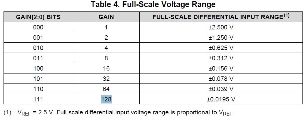
on the datasheet, it says it has a lower input range of +/- 7mV. I am kind of confused on how you got that lower input range and what it is actually referring too. Is it the actual range from AINP and AINN?

-
Ask a related question
What is a related question?A related question is a question created from another question. When the related question is created, it will be automatically linked to the original question.