This thread has been locked.

If you have a related question, please click the "Ask a related question" button in the top right corner. The newly created question will be automatically linked to this question.

ADS1262: PCB Layout verification to ensure lowest possible noise.

Part Number: ADS1262

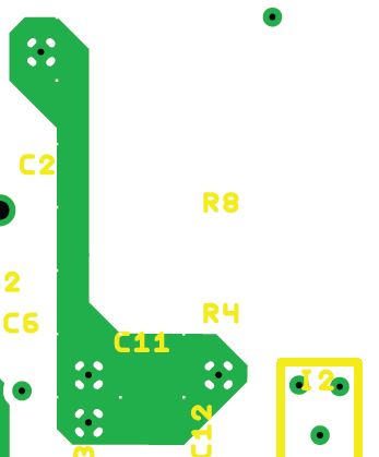
I have attached a schematic of what we call our "detector board".  This board will have a photodiode on it which will send its signal output directly into an op amp, which we use for amplification if needed as well as a filtering.  We utilize the highness filter and the lowpass filter in scenarios where we modulate the light source so the that detector output is a sine wave and we can run FFT on this signal.  In other applications, we only utilize the lowpass filter for a constant on light source so the detector output is DC.  I am looking for a quick check of our layout so that we have confidence about proceeding with this design.

Thanks,

AndrewTop_Copper.pdfPD32B_Schematic.pdfInner_Upper_GND.pdfInner_Lower.pdfBottom_Copper.pdf

  • Hi Andrew,

    Welcome to the TI E2E Forums! Overall the layout looks pretty good. I just have a few comments:

    1. DGND could have a shorter connection to GND here...I don't see a need to elongate this connection by routing through the bottom layer. Refer to this FAQ for additional details why I recommend connecting DGND directly to GND.

    2. You have a lot of empty space on every layer where you could include a ground plane fill. The more metal you use for the GND plane, the lower its impedance will be. Just take care to add vias all across the PCB to connect the grounds planes between layers.

    3. You have series resistors on a few of the SPI signals, which is a great idea! I would just recommend adding a series resistor to the SCLK trace, since this signal switches more frequently than all of the others. The series resistor can help slow down the edge and prevent ringing on this trace.

  • Chris,

    Thanks for the quick feedback. We will actually be communicating with multiple of these "detector boards", so on the main board, we added the series resistor on the clock line there since it would be the same for all detector boards. I will look into your grounding suggestions and let you know if I have any questions.

    Thanks.