This thread has been locked.

If you have a related question, please click the "Ask a related question" button in the top right corner. The newly created question will be automatically linked to this question.

ADS1293: Switching RLD on increases system noise

Part Number: ADS1293

Hi all,

I was performing a test according to standard 60601-2-47 chapter "201.12.4.4.106 System noise". I am using two inputs in my setup.

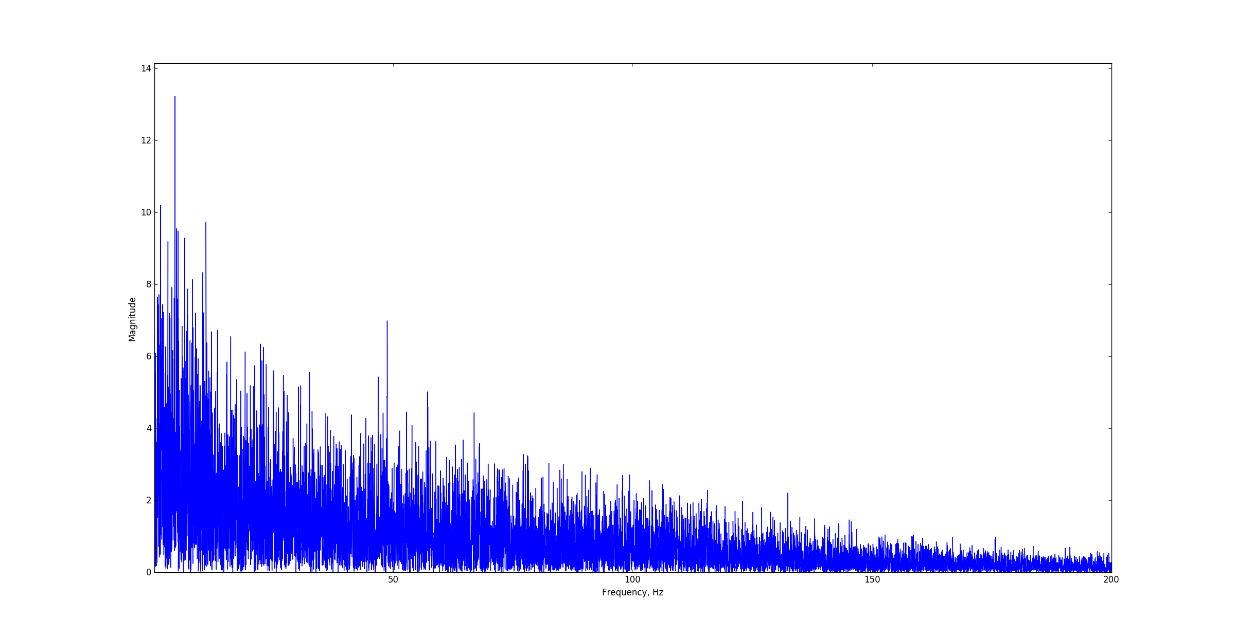
When I don't enable RLD, I get ~10uVp-p noise, but when I enable RLD on one of the two inputs, I get much larger noise - about 80uVp-p this is much bigger than 50uVp-p quoted in the standard. How come RLD injects so much noise? Can I avoid it? I am attaching all the related info I have.

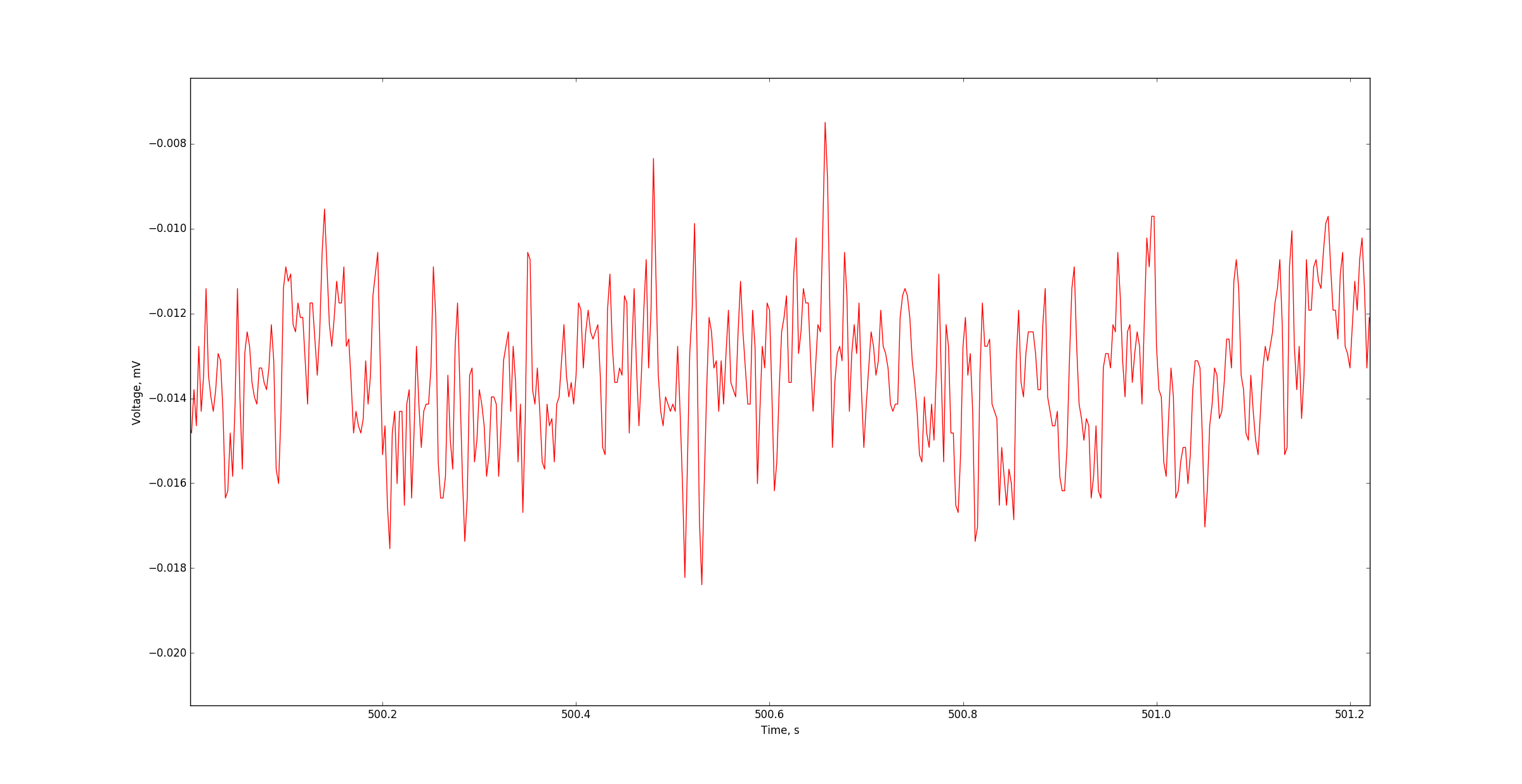
System noise with RLD off:

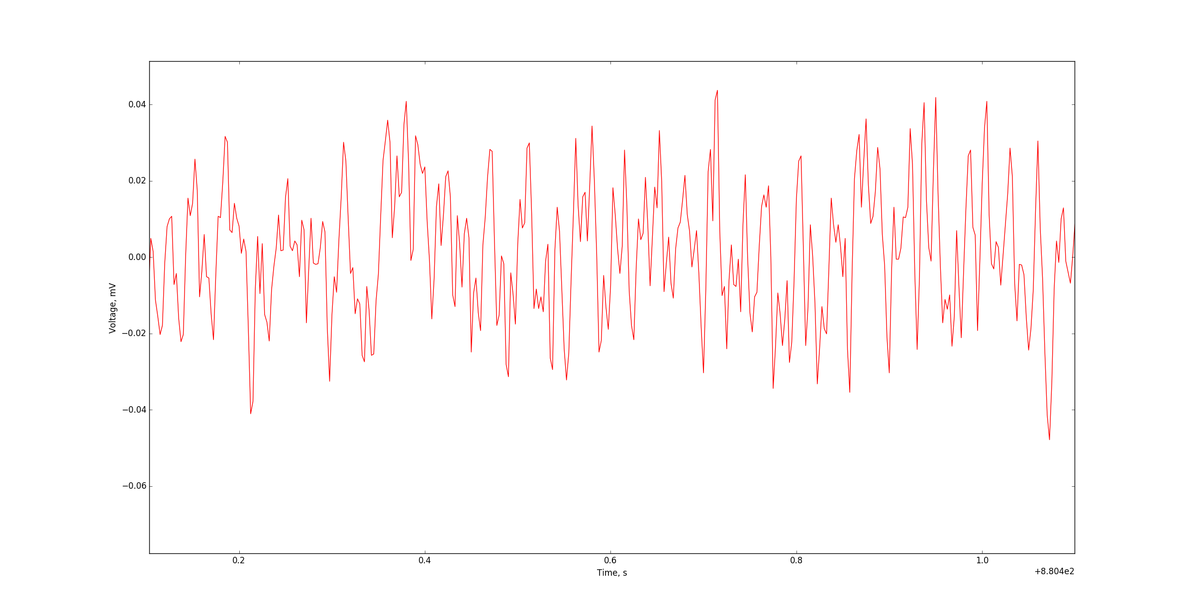
System noise with RLD on:

Schematics:

ADS1293 config:

        {FLEX_CH1_CN, 0b00011010}, //0x01 POS - IN3, NEG - IN2
        {FLEX_CH2_CN, 0x00}, //0x02
        {FLEX_CH3_CN, 0x00}, //0x03
        {LOD_CN, 0b00001000}, //0x06  DC lead off detection - OFF
        {LOD_EN, 0x02}, //0x07 lead off detection on IN2
        {CMDET_EN, 0b00000000}, //0x0a CM detection - OFF 
        {RLD_CN, 0b01110011}, //0x0c high BW, high cap dirve RLD on IN3
        {AFE_RES, 0x09}, //0x13 high res 200kHz for channel 1
        {AFE_SHDN_CN, 0b00110110}, //0x14 insta and modulator shutdown for ch2 and ch3
        {CH_CNFG, 0x00}, //0x2f
        {R2_RATE, 0x01}, //0x21 R2=4
        {R3_RATE_CH1, 0x40}, //0x22 R3=64 400 samples/s 80Hz BW ADCmax = 0x800000
        {R3_RATE_CH2, 0x01}, //0x23
        {R3_RATE_CH3, 0x01}, //0x24
        {R1_RATE, 0x01}, //0x25 R1=2 double pace rate for CH1
        {DRDYB_SRC, 0x08}, //0x27 ch1 as DRDYB source
    {FLEX_PACE_CN, 0x00}, //0x04
    {FLEX_VBAT_CN, 0x00}, //0x05
    {LOD_CURRENT, 0x0f}, //0x08
    {LOD_AC_CN, 0x00}, //0x09
    {CMDET_CN, 0x00}, //0x0b
    {WILSON_EN1, 0x00}, //0x0d
    {WILSON_EN2, 0x00}, //0x0e
    {WILSON_EN3, 0x00}, //0x0f
    {WILSON_CN, 0x00}, //0x10
    {REF_CN, 0x00}, //0x11
    {OSC_CN, 0x06}, //0x12
    {AFE_FAULT_CN, 0x06}, //0x15 disable fault detection for CH2 and CH3
    {AFE_PACE_CN, 0x01}, //0x17 analog pace shutdown
    {DIGO_STRENGTH, 0x00}, //0x1F
    {DIS_EFILTER, 0x06}, //0x26 filter disabled for CH2 and CH3
    {SYNCB_CN, 0x00}, //0x28
    {MASK_DRDYB, 0x00}, //0x29
    {MASK_ERR, 0xff}, //0x2a
    {ALARM_FILTER, 0xFF}, //0x2e


  • Hello Albertas,

    Thank you for your post!

    Could you elaborate more on the electrode configuration during the test setup? Ideally, the electrodes should be shorted together and tied to the RLD output. This keeps the electrodes from floating and ensures that any noise remains common to both inputs.

    When you say "enable RLD on one of the two inputs," are you changing a register setting? Can you specify the address and the setting before and after?

    Lastly, it may be more telling if you can compute an FFT on the raw data and look at the frequency content of the noise. This may tell you if it's just power-line noise coupling or perhaps other signals on the board. Do you have the raw data in a text file that you can share? Either decimal or hexadecimal format is fine.

    Best regards,
  • Hi Ryan thanks for your answer,

    I am using two inputs. Both of them are connected to ads1293 converter as two inputs on channel 1. I am shorting both inputs together as specified in the standard - using 51k and 47n in parallel in series to each input. Then I make two separate measurements switching RLD on one of the inputs - with RLD enabled RLD_CN=0b01000011 and RLD disabled RLD_CN=0b01000000. All my other configuration setting are in the previous post.

    In the measurement with RLD enabled I get much higher noise. I have calculated FFTs of both signals. First no RLD:

    With RLD ON:

    I am attaching raw data I acquired. The data in files is voltages in millivolts, I calculated them from raw adc values using this formula:

    ADCmax=0x800000
    Vref=2.5
    
    b = (a - ADCmax/2)*2*Vref/ADCmax/3.5*1000
    

    Let me know what can I do to make things more clear.

    noise-floor-DC-coupled-RLD-OFF.txt

    noise-floor-DC-coupled-RLD-ON.txt

  • Hi Ryan,

    Any update on this?

  • Hi Albertas,

    Thanks for the raw data and FFT plots. I understand what you are doing now.

    Channel 1 is always configured as IN3 - IN2. Each input has an additional 47n || 51k impedance in series after the connectors (J4 and J3, respectively). When you change the RLD_CN register setting, you are now shorting RLDOUT to IN3 inside the ADS1293. This is going to give you terrible noise results as the two input paths no longer see the same impedance. The result is poor CMRR, which converts the common-mode noise to a differnetial noise.

    What you want to do instead is keep J4 and J3 externally shorted via the 47nF || 51k imepdances and attach a third electrode from RLDOUT through another 47nF || 51k impedance. The driven output from the RLD amplifier will then be common to both IN3 and IN2.

    Was this the way you intended to test the noise performance, or did you, by chance, intend to experiment with how the common-mode signal was derived? in the CMDET_EN register (0x0A), you can select up to 6 individual electrode inputs to be used in deriving the common-mode signal for RLD. The RLD amplifier is configured in an inverting amplifier configuration to create a cancellation signal at the output.

    Best regards,