This thread has been locked.

If you have a related question, please click the "Ask a related question" button in the top right corner. The newly created question will be automatically linked to this question.

ADS54J66: SPI, 24b vs 32b, page selection and EVM config files.

Part Number: ADS54J66
Other Parts Discussed in Thread: LMK04828

Hi Jim,

Still working on the ADS54J66. My goal is program my ADC over spi directly, but the address paging doesn't seem to agree with the .cfg files provided in the evm.

For the EVM, we were given this set of config files for use with the evm program tool:

""

ADS54Jxx_ANALOG
0x0000 0x81
0x8039 0xC0 // always write a 11 to bits 6-7
0x8053 0x80 // divide by 2 required for ADS54J66
0x8055 0x00 // must write 0
0x8056 0x00 // must write 0
0x8059 0x20 // must write a 1 to bit 5
ADS54Jxx_DIGITAL
0x6800f7 0x01 //digital top reset
0x680000 0x01 //reset digital
0x680000 0x00 //clear reset
0x614100 0x02 // dec filter page mode 2
0x614101 0x00 // 0 for LPF, 1 for HPF CHB & C
0x614102 0x00 // bit 5, 0 for LPF, 1 for HPF CHA & D
0x690000 0xC0 //set CTRL K + control mode
0x690001 0x02 // JESD mode 40X
0x690006 0x04 //set K to 5
0x6A0016 0x02 // JESD PLL Mode 40x data sheet typo???
0x6A0017 0x40 // PLL reset
0x6A0017 0x00 // PLL reset release
ADS54Jxx_LOWLEVEL
0x4004 0x69
0x4003 0x00
0x4005 0x01 // disable broadcast mode

"" You can see the full file attached below. 

Where the address is in column 1 and the data is in col 2. This works great for us when using the gui.

However, this cfg seems to not be a bit accurate representation of what is being sent out over the spi line to the ADC. In the data sheet, a single spi transaction is 3 bytes, 24b long, where this shows an extra address byte in the digital config. I know there's page access writes, which appear to be being abstracted by the ADS gui. I cannot probe the spi lines directly b/c the EVM doesn't have test points. 

Is there a way to get a bit accurate representation of whats going on here? Or, put another way, how can I translate the above file into spi transactions that are only 24b long?

Thanks for the help,

    -Jake 


ADC_Config.cfg

  • Hi Jake
    I have notified Jim regarding your latest question.
    He will review the information and respond soon.
    Best regards,
    Jim B
  • Jake,

    The GUI and the configuration files it use works as follows:

    ADS54Jxx_ANALOG

    0x8053 0x81


    The ADS54Jxx_ANALOG GUI command will write two 24 bit words for every data line below it. The first word will always use 0x11 for the address and use the upper two bytes of the address value in the data entry line for the data. The address is first (4 bytes), followed by the data (2 bytes) in the data entry line. For the example above, a data value of 0x80 will be written to address 0x11. This will set the page for the next write.


    The second write will use 0x00 for the upper address bits and

    A7-A0 and D7-D0 from the data entry line. For the example above, a data vale of 0x81 will be written to address 0x53. This will continue for all line entries under ADS54Jxx_ANALOG


    ADS54Jxx_DIGITAL

     0x6800F7 0x01


    The ADS54Jxx_DIGITAL GUI command will write four 24 bit words for every line below it. The first word will always use 0x4003 for the address and the middle two bytes of the address data entry for the data.


    The second word will always use 0x4004 for the address and the upper two bytes of the address entry for the data.


    The third word will always be 0x60 for the upper address bits, A7-A0 of the address value for the lower address bits and D7-D0 for the data. This is a write to CHA.


    The fourth word will always be 0x70 for the upper address bits, A7-A0 for the address value for the lower address bits and D7-D0 for the data. This is a write to CHB. The writes to the ADC will look as follows with this example:


    0x4003 0x00   //Write 00 to LSB byte of page address 

    0x4004 0x68 // Write 68 to MSB byte of page address

    0x60F7 0x01  // Write 01 to address 0xF7 of channel A ( R/W = 0, M = 1, P = 1, CH = 0 )

    0x70F7 0x01  // Write 01 to address 0xF7 of channel B ( R/W = 0, M = 1, P = 1, CH = 0 )


    Hope this helps.


    Regards,


    Jim


  • Hi Jim,

    It's an odd format, but I think I can use that to translate what you've given me. What about the //ADS54Jxx_LOWLEVEL registers? Do they have any special gui injections?

    Would you by chance have a plain copy or example of spi writes that actually program this device?

    Thanks,
    -Jake
  • Hi Jim,

    Let's say I wanted to read the address from the analog page from the cfg as shown in my first post.
    0x8039 0xC0
    becomes
    0x0011 0x80
    0x0039 0xC0
    to write to the address.

    And to read, I think I want to do
    0x8039 0x00

    But what happens if instead I perform a read operation on both the page selection and the data transaction?
    0x8011 x00
    0x8039 0x00

    Thanks for the help
    -Jake
  • 7608.SPI writes.docxJake,

    The low level command writes the address and data as is. This will use send the address 4 bytes first followed by the two bytes of the data value. See attached. This also shows an example of a read command.

    Regards,

    Jim


  • Hi Jim,

    Thanks for the help. I'm now able to read and write to the analog page.

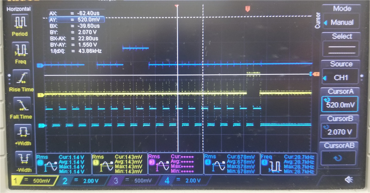
    However, I'm unable to use your commands to read from any of the digital registers. Additionally, my ADC only appears to be writing high to about 500mV. I've checked my supplies and they are all good, and nothing else is on the spi line to cause any issues. Is this something you've seen before?

    Thanks,

       -Jake 

  • Jake,

    You must have both the ADC clock and SYSREF running before the SPI will work properly. After writing to the digital registers, you must pulse the digital reset before these will load. This is address 0x00, bit 0 in page 0x6800.

    Regards,

    Jim

  • Hi Jim,

    Thanks, I'm investigating this further. I've supplied the ADC clock, and wrote the proper digital reset bit, and I can now read and write to any register. I triggered sysref over spi via the method described in section 9.3.2.1.1 of the lmk04828 datasheet. However, I'm still having the 500mV issue.
    I know my power sequencing may be an issue right now (which I'm going to try and fix tomorrow). However, that should just effect the default registers correct? Or does that entirely wreck all known behavior?
    I'm pretty stuck on this read back right now, since it requires me manually decoding over a scope instead of with my logic analyzer

    Thanks for all the help,
    -Jake
  • Jake,

    What do you mean when you mention "  my ADC only appears to be writing high to about 500mV"? Are you referring to the digital output bits? The first thing I would do is to monitor the current drawn by the ADC. Power down ADC using SPI and verify the current drops. This will verify the SPI is working without using read back mode.

    Jim

  • Hi Jim,

    Yes, I mean the SPI MISO line is only being driven to 500mV instead of the 1.8V I expect. I powered down the ADC with SPI and watched my current drop by 400-500mA. I can trigger a read on SPI, and based on scope samples, it matches what I have programmed, but the amplitude of those readbacks is only 500mV.

    My clock rate is only about 80kHz on SPI, and I've tried adding different loading resistors to the line to check it's not a weird issue with termination. There is no change to the signal amplitudes.

    I need SPI readback to monitor the status registers for bringing up the JESD lanes.

    Thanks,
    -Jake
  • Jake,

    I assume you are referring to the SDOUT pin, correct? The level of this signal should typically be at DVDD. Is your DVDD supply at 1.9V? What are you driving with this signal?

    Regards,

    Jim

  • Hi Jim,

    I've figured out what the issue is, I just don't know how to solve it. My DVDD line is 1.8V

    The ADC's won't release the MISO line after their CS has been pulled up.

    I have 4 hooked up right now on the same line, and they all try to pull down. When I power them up individually, they work great and output as expected. But put them all on the line, and they'll fight the others when they try to speak (even when the CS lines are distributed properly). I can also verify the MISO line is not going HI-Z by tying a 1k resistor from 1.8V to MISO. The line remains at 0V, indicating it's not high impedance.

    Is there a configuration register I've missed for these devices to become compliant? I've checked my spi exactly matches the timing diagram given in the sheet. I've heard of things like sending a few extra clock cycles through the device after CS has been raised?

    Thanks,
    -Jake
  • Jake,

    The output is either active or driven low. There is no way to tri-state this signal.

    Regards,

    Jim