Other Parts Discussed in Thread: ADS131A04
Hello,
I am supporting a customer who is using the ADS131A04EVM to interface it with an FPGA and has some issues with the startup procedure.
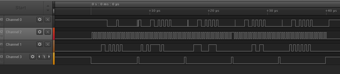
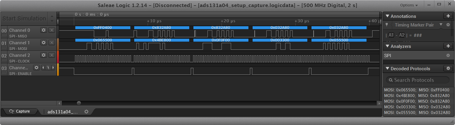
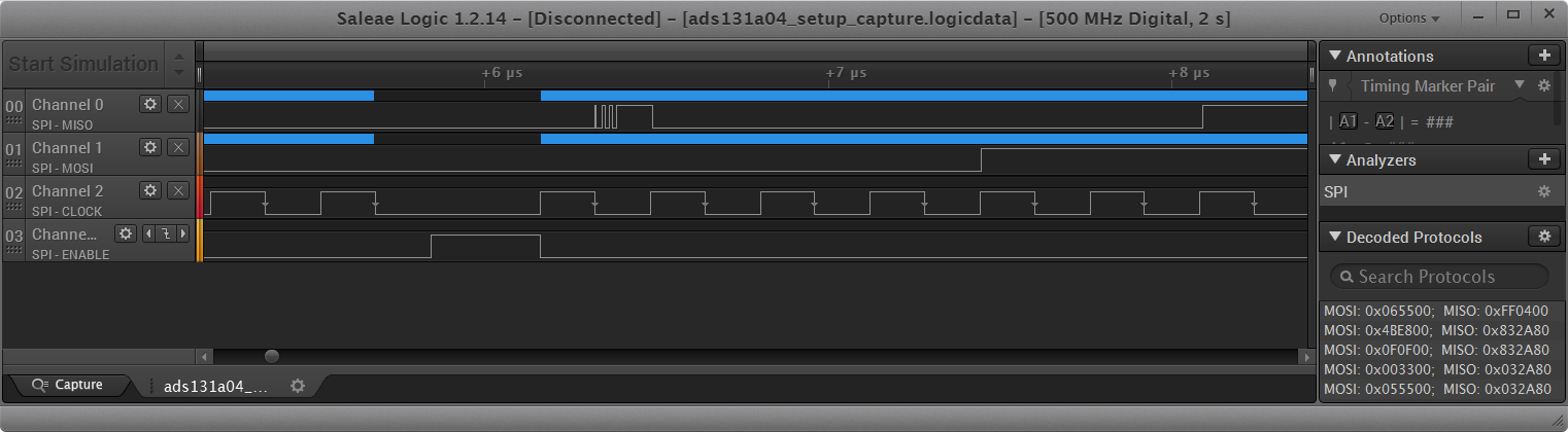
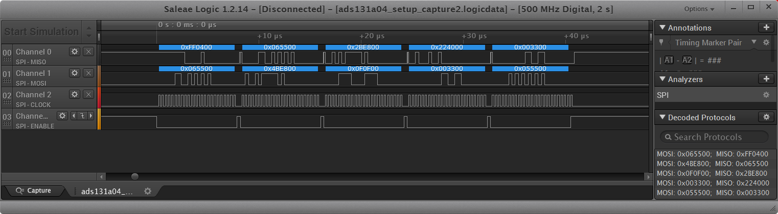
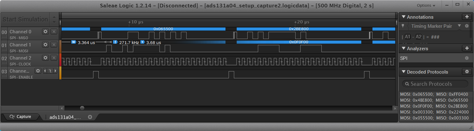
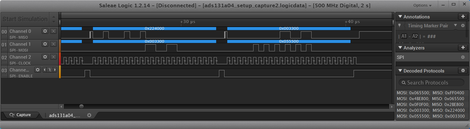
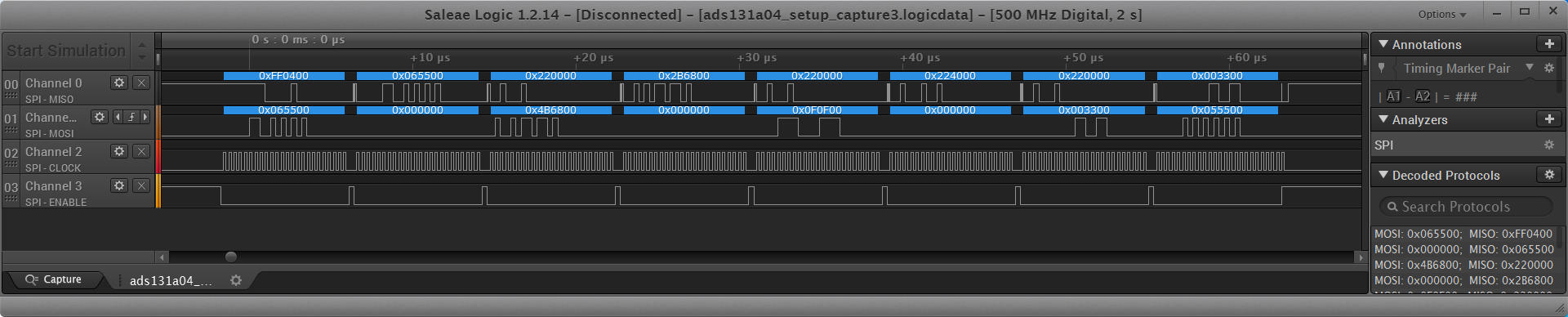
In the capture below he is attempting to follow that procedure (listed in page 79 of the ADS131A04 datasheet) and makes the following observations:
- He sees the ready status
- He sends the unlock command
- He sees the unlock command was received in the status word of the next write
- However, after that, all config writes only get back the unlock status word on the DOUT line
- He also sees a little pulse on the DOUT line on the next command frame start
The clock period used was of 320ns and the channels visible in the capture below are as follows:
- Chan 0 – miso (DOUT)
- Chan 2 – clock
- Chan 1 – mosi(IDN)
- Chan 3 – cs

The steps that were followed are the following (DIN = falling edge, DOUT = rising edge):
- Send Unlock command – 0x065500
- Write to A_SYS_CFG register – 0x4BE800
- Write to ADC_ENA register – 0x0F0F00
- Send Wakeup command – 0x003300
- Send Lock command – 0x055500
In terms of hardware, he has an FPGA eval board connected to the SPI header of the ADS131A04EVM, with mosi and miso (per silkscreen issue) swapped and the evm digital side spi traces cut to isolate for external use only. The jumper settings on the EVM are as follows:
- M0 – IOVDD
- M1 – GND
- M2 - GND
- S4 – down (manual)
- S5 – up (header)
- S8 – up (header)
- S7 – down (slave)
- JP8 – uninstalled
- JP9 – installed
- JP10 – uninstalled
Any idea why the second step isn't working and why DOUT repeatedly shows the unlock status word after a quick pulse?
Thanks.