This thread has been locked.

If you have a related question, please click the "Ask a related question" button in the top right corner. The newly created question will be automatically linked to this question.

ADS131A02: DRDY data line not behaving as expected

Part Number: ADS131A02
Other Parts Discussed in Thread: TMS320C5535, , ADS131A04EVM

I'm currently trying to receive data from the ADS131A02DC, but am having a problem with the DRDY line. My hardware is set up such that M0 is HIGH (asynchronous interrupt mode), M1 is HIGH (32 bit), and M2 is LOW (hamming disabled). I've managed to successfully write and read to the ADC registers and have read the STAT_M2 register to verify that my hardware is setup correctly (it is). 

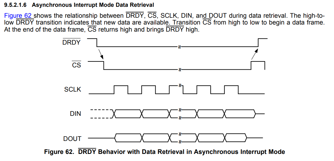
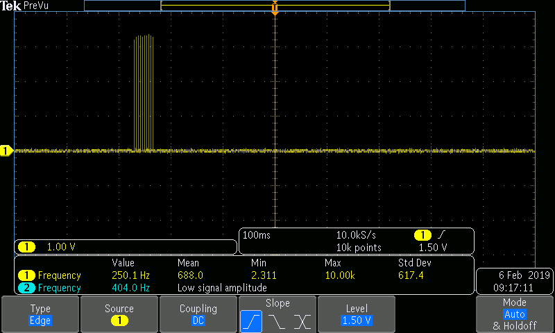
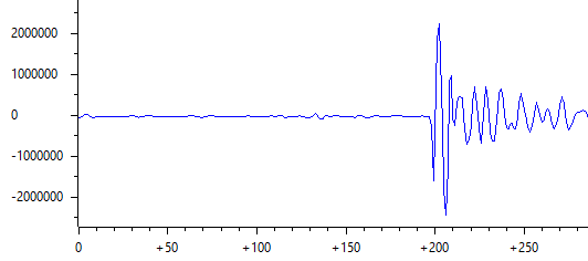
The DRDY line is suppose to be active low so I expect the voltage to be HIGH at 3.3V, but I'm seeing the following on the oscilloscope even though the ADC is in STANDBY MODE:

I was worried that the DRDY line needs to be driven with a pull-up resistor, so I attached a pull-up resistor to 3.3V but the problem persists. I have removed the pull-up resistor and am unsure what else could be wrong. 

Communication is working fine, so I'm assuming DIN/DOUT/SCLK/*CS are all OK.

*RESET is pulled HIGH(3.3V)

*DONE is OPEN, but internally pulled-up HIGH(3.3V) within the ADC.

*DRDY is OPEN, for probing purposes. I expect a HIGH signal but am getting the signal shown above. 

Any guidance and help would be greatly appreciated. 

  • Eddie,


    Thanks for your post. Based on your write up I was unclear about the problem that you were seeing. Are you concerned that the /DRDY is often low? The act of /DRDY transitioning low indicates a new conversion is ready and it is not the level of /DRDY that indicates the conversion. You can see this in Figure 4 or 5 of the datasheet, where the /DRDY pulses for each conversion completion. I would have expected the /DRDY to give a similar pulse train as you see in the oscilloscope plot when in operation. The line is actively driven, so you shouldn't need a pull-up.

    However during standby mode, the device shouldn't be doing any conversions and I would expect /DRDY to be idle. I'm not sure if you've momentarily set the device into standby and then brought it back with a wake-up, but that's what it looks like on the plot.

    Hopefully my comments cleared up the behavior of /DRDY. If I've misunderstood your post about /DRDY, post back and we can discuss it.


    Joseph Wu
  • Joseph, 

    Thank you for getting back to me and clarifying some details about the data line. I do have two follow-up questions: 

    1) The DRDY signal in the oscilloscope plot you see above begins occurring as soon as the IC starts-up. I never unlock the device or take it out of standby mode. So shouldn't the DRDY be idle at HIGH like you mentioned? 

    2) Is the DRDY signal in the oscilloscope plot somehow inverted? The datasheet says that *DRDY is active low, so I would have expected the signal to start HIGH, go LOW, then HIGH again. Instead, the signal seems to start LOW, go HIGH, then go LOW again. 

    EDIT:

    *DRDY does not seem to behave as expected, even when in active mode. Here are the steps I take:

    1) Turn on the IC. *DRDY outputs the signal shown in the first oscilloscope plot posted above (see original question post). 

    2) Send UNLOCK command. UNLOCK command was acknowledged. 

    3) Configure the registers as follows: 

    // HRM set to low power mode because f_MOD is going to be set to < 1.05MHz
    #define INIT_A_SYS_CFG  0x20
    
    // Set ICLK = CLKIN/2 = 16.384MHz/2 = 8.192MHz
    #define INIT_CLK1       0x02
    
    // Set fMod = ICLK/8 = 8.192MHz/8 = 1.024MHz
    // Set fDATA = fMod/4096 = 0.250KHz
    #define INIT_CLK2       0x80

    Received successful acknowledgment on all these writes. 

    4)  Write 0x0F to ADC_ENA (address = 0Fh). Write was acknowledged. 

    5) Send WAKEUP command. WAKEUP command was acknowledged. *DRDY shows: 

    NOTE: This is a periodic signal which occurs approx. every 4s. 

    6) Send STANDBY command. STANDBY command was acknowledged. *DRDY shows: 

    NOTE: This is a periodic signal which occurs approx. every 4s. 

    6) Send LOCK command. LOCK command was acknowledged.

    I don't think the plot in step 5 is correct. I updated the registers to have the ADC output at 0.250KHz. However, the *DRDY line in the plot does not seem to be operating at the frequency.

    I also don't think the plot in step 6 is correct. I would have expected *DRDY to idle HIGH during standby mode. 

    Any help and guidance would be appreciated. 

    Best, 

    Eddie

  • Eddie,


    We have an ADS131E04EVM and I had to test out the device to see what it does at start up. When I plug it in to start up, it does start with the /DRDY high. When in operation, the /DRDY will spend most of the time high because it follows the /CS high after configuation and reading the device.

    When I look at the EVM /DRDY, the device comes up active. There is already a periodic /DRDY indication. For each one of these /DRDY transitions low, the EVM responds by sending a null command, and the device responds with an FF04 (for your device, you would get the FF02). If there hasn't been a setup, then it means the device comes up active. Then for the EVM, I still need to do an UNLOCK, WAKEUP, and then WREG for 0F 0F to enable the ADCs.

    For your setup, it does seem like the oscilloscope plot is inverted. However, you might get the same thing if you left the /CS low after sending the first commands. The /DRDY would appear as pulses and idle low.

    I'll look through your setup and ask a couple of engineers that have a bit more experience with this particular device and I'll get back to you.


    Joseph Wu
  • Joseph, 

    I appreciate you bearing with me.  

    I thought your theory about *CS being low and thus making *DRDY low was possible, so I decided to take a look at that on the O-scope. This is the plot as soon as I turn on the IC: 

    YELLOW: *DRDY

    BLUE: *CS

    PURPLE: SCLK

    I'm using TI's TMS320C5535 to talk to the ADC. Notice that *CS is LOW. This is because the SPI peripheral in the processor is NOT configured yet: 

    However, the ADC is sending period *DRDY signals. It should be HIGH at start-up.

    After the SPI peripheral in the processor is configured, I get the following when writing and reading to/from the ADC registers: 

    As you can see, *CS is configured correctly (active low). The clock polarity is LOW at idle, and MOSI/MISO is sent on the clocks rising edge ( which agrees with how the datasheet says the ADC SPI settings should be).

    It's strange that *DRDY STILL seems to be inverted, even though *CS is HIGH. It's also strange that *DRDY has a much longer frame than *CS. I assumed it should follow the *CS line pretty closely.

    Is *DRDY  suppose to be triggering when I read/write to the registers? The datasheet says it only goes low when conversion data is ready, NOT when SPI data is ready. The datasheet isn't clear on this. 

    EDIT: 

    I set up an interrupt on the processor to trigger at the falling edge of the *DRDY line after I put the ADC in active mode.

    I then read incoming data from DOUT (32-bit STATUS, 32-bit Channel 1 Data, 32-bit Channel 2 data). The STATUS data (STAT_1 Register) is a value of 0x02, which indicates that there is a data ready fault.

    I suppose this is to be expected, considering *DRDY is inverted. I'm not sure what else I can change to the system, it seems that the inverted *DRDY line is the reason I cannot get conversion data and line is not behaving according to the datasheet. 

    Best, 

    Eddie 

  • Eddie,

    Sorry I didn't get back to you earlier. It took me a bit to get something together.

    I was able to get an ADS131A04EVM to look at the device response (it should be the same as the ADS131A02). I used a logic analyzer to look at the startup waveforms and they basically look the way I expect. Here's a plot:

    When the device powers up, the starts the /DRDY, but the master starts with /CS low. In this case, it looks like the pulse train that I expect.

    After power up there are a few /DRDY pulses and then the master finally responds, but I think all it is providing at this point is null commands. The master then skips responses for a couple of /DRDY pulses and the device returns to the remaining pulse train. To me that was the part I wasn't sure about, but it's not completely unexpected. Without any /CS transition, there's nothing to return /DRDY high except for the completion of a conversion.

    After that, the device responds with a null command for each /DRDY and then you see the /DRDY mostly high.

    For your device, It seems like a similar response. The only thing that I found to be different is that your data period is a little different. In one of the scope shots where you first write and read from the ADC registers, it looks like you're missing a few /DRDY pulses (that is if you haven't changed the data rate).

    Note, I'm not sure if my logic analyzer is able to give the time resolution to decode everything sent to the device. I tried pulling out the SPI, but it looks like I'm sending way too few bits for each transaction. Let me know if this helped you in any way.

    Joseph Wu

  • Joseph, 

    That logic analyzer data was very useful. I programmed the DSP to respond with a NULL command every time it sees that falling edge on *DRDY, and managed to get a similar signal to the one you show above. I have assumed that the *DRDY line is working as intended, and I have now moved one to trying to collect data from the ADS131A02. 

    My ADC setup is sampling a differential signal which contains a 2.5V common mode offset at a range of 0-5V. Following the same steps I've posted above to get the ADC into active mode, I get the following numbers from the ADC: 


    My signal was initially idle, which is reflected in the plot above (before sample ~65). Then my analog signal does change by about 1V. The plot above seems to be corrupted data, and it may have to do with my SPI setup. Here are my questions: 

    1) 

    I currently have the ADC to be setup as dynamic frame size(CRC disabled). However, this version of the ADC has 2 channels, not 4. Should I be talking to the ADS131A02 with a frame size of 5 (status, channels 1 - 4) or a frame size of 3(status, channels 1-2)? 

    I've already tried communicating with both setups, but get the same corrupted plot with both. 

    2) The datasheet has no mention of the output format of the ADC. Is it a 24bit signed or unsigned number? 

    I'm still in the process of debugging, and will let you know if I have any further questions. 

    Best, 

    Eddie

  • Eddie,


    1. With the ADS131A02, you would use the frame size of 3. In dynamic-frame mode, the number of device words per data frame is dependent on if the ADCs are enabled and if the CRC data word is enabled. In this device, there are only two ADCs enabled and in your example CRC is disabled. This gives the status word, and the data from two channels.

    2. The output data format for the ADC is two's complement notation for negative numbers. This is discussed in the Data Words section of the datasheet on page 38. Because negative numbers are represented in this way, this might explain some of the large numbers that you see with the data you show in the graph. If you can collect a file with the data and post it here, I can help you make the conversion.


    Joseph Wu
  • Joseph, 

    I managed to get this (relativity) beautiful signal sampled using a low data rate:

    It checks out with what I expect. Thank you for bearing with me and taking your time to clarify things for me, I really appreciate it!

    Best, 

    Eddie

  • Eddie,


    That's great. I'm glad you got it working with some reasonable data output.

    If you have any other questions, feel free to post back.


    Joseph Wu