This thread has been locked.

If you have a related question, please click the "Ask a related question" button in the top right corner. The newly created question will be automatically linked to this question.

RE: ADS114S08: Data output from ADC shows unexpected offset

Other Parts Discussed in Thread: ADS114S08

Dear Bob,

You are right about the power supply noise. Our SMPS was very noisy we replace it and all problems were resolved. Also the STATUS register which we were getting spurious values also stopped. Found very stable readings and spurious zero voltage given by adc also stopped.

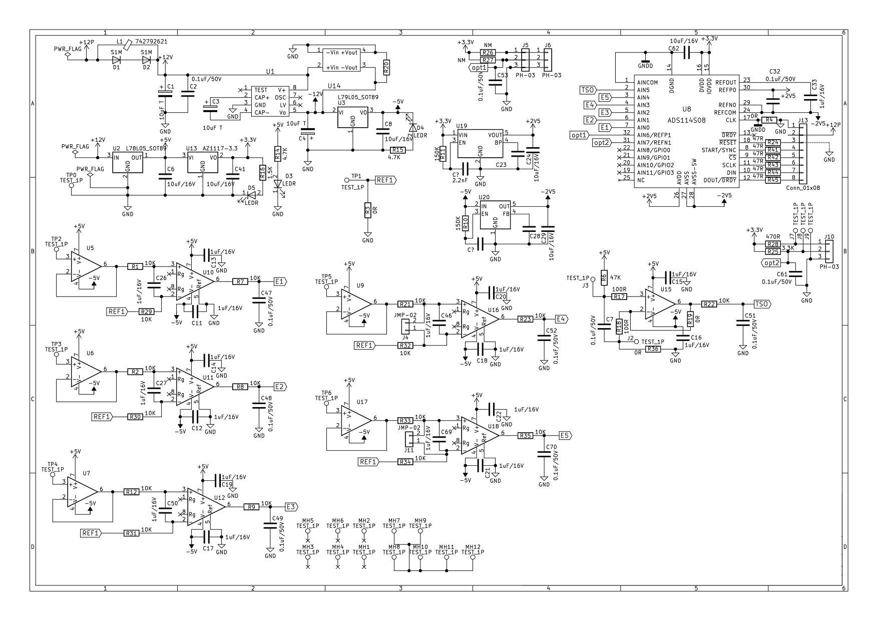
Have attached our schematic for your reference do give your suggestion if any change is required. 

One more point is when we give -0.34volt to TP2 we get -1.68volt (gain of 5 of opamp stage 2) at E1 point . But output given by ADC is -0.3131volt. i.e. we are getting offset of 0.028volt. Same for positive voltage. 

Please advice why this offset of 20-30milli volt is seen.  

Thank you.

  • Hi Amol,

    I split the thread from the previous posting as the topic has changed. There are several things that are not clear. From your schematic it appears that you have a small signal that is buffered, followed by an external gain stage (approximately 5) that is then converted by the ADC. You then calculate the result by dividing by the ADC result. I see that there is a potential gain error as you are assuming that the buffer has no offset or gain issues and that the gain stage is exactly 5. From reverse calculation (1.68/0.34) we see it is 4.941.

    It would be very helpful to know the raw code from the ADC prior to any calculations. If the input voltage is 1.68V, then I would expect an output code of approximately 11010 codes (0x2B02). With the PGA bypassed, there might be a voltage drop across the series input resistor (R7) that may be causing some of the offset you are seeing, but this would be in uV and not mV.

    Based on the added external gain, I will assume that the maximum sensor voltage is +/- 500mV. This is an assumption and the sensor output may be smaller. Depending on the sensor output voltage you may be able to enable the PGA on the ADS114S08. In this case you should be able to remove the buffer and the external amplifier stage and measure the sensor voltage directly. I would also suggest that you can use the internal 2.5V reference of the ADS114S08 for a full-scale range of +/-2.5V instead of the REF0 which is set at a full-scale range of +/-5V. Using the 2.5V reference will improve the dynamic range.

    Instead of a gain of 5 you can set the ADS114S08 to a gain of 4. The output result will not need any further computation. This will remove the error associated with that external amp. You will also improve input referred noise using this the internal PGA.

    If there is something I'm not seeing please let me know. In particular the full output range of the sensor and the required resolution. I would still suggest with even the current configuration that you would change the reference to the internal reference as you are making your measurement to AINCOM (which is connected to GND and making the maximum input voltage range +/-2.5V). If you must use the 5V reference created at REF0, then turn off the REFP and REFN reference buffers (as opposed to just the REFN).

    One other thing I noticed that may or may not be an issue is that the ground connected to AINCOM has a different symbol and net name than all the rest of the ground pins. If the ground connected at AINCOM has a much different path than the ground at the sensor input, this may also affect the measurement.

    Best regards,
    Bob B