This thread has been locked.

If you have a related question, please click the "Ask a related question" button in the top right corner. The newly created question will be automatically linked to this question.

DAC38RF80EVM: System Clock Configuration

Part Number: DAC38RF80EVM
Other Parts Discussed in Thread: LMX2595, LMX2595EVM, LMK04828

Hey,

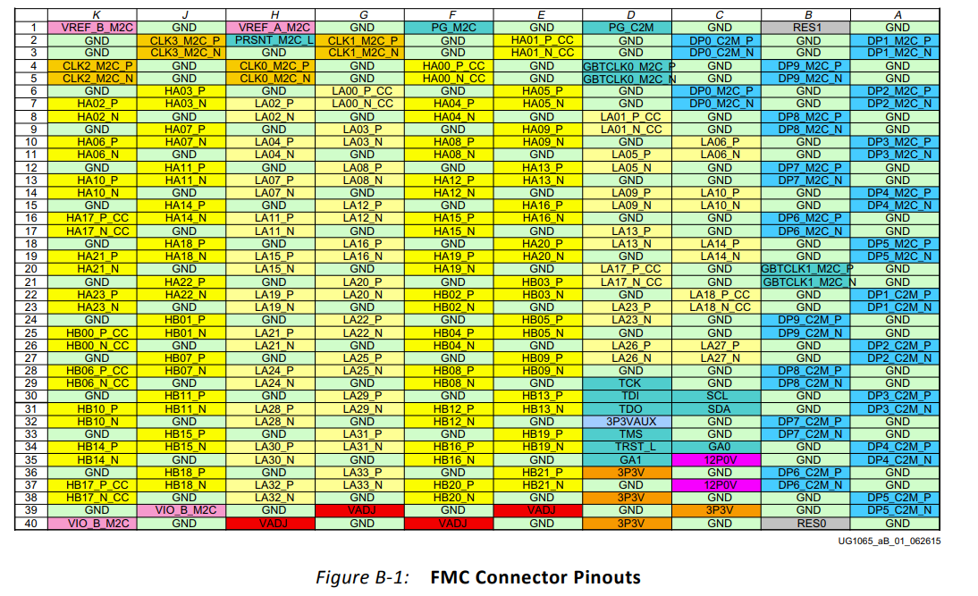
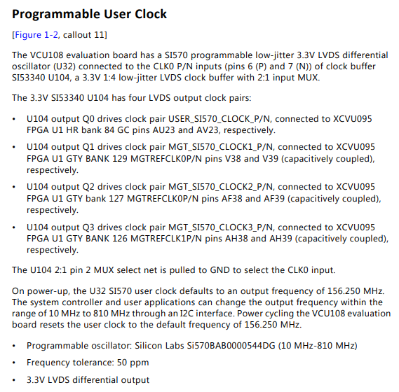
Our current system setup consists of a DAC38RF80EVM digital to analog converter, and LMX2595EVM clock synthesizer, and a Xilinx VCU108 FPGA board. My original intent was to use the LMX2595 as the master device clock for both the FPGA and the DAC (with modifications for differential clocking)  dividing the clock to the correct frequency for the FPGA clock per the system parameters (line rate, lanes, etc.). However, the SMA input clock on the FPGA cannot be used for the FMC connector based on my reading. I've also looked into trying to use the user programmable clock on the FPGA as an oscillator input to the LMX2595 so that the system still shares a common clock, but there are no output terminals on the FPGA clock to tap into to send that signal to the LMX2595. It also appears that the FMC clock pins on the DAC (J2/3 or K4/5)and FPGA(G2/3 or H4/5) don't line up to transfer any clocks from one device to the other in either direction. 

So my question here is, am I missing something here or did I simply choose two incompatible devices? I know that they have to share some kind of common source even if the clocks going into each are at different frequencies, but I can't seem to think of any other methods by which to do so though with my current setup. 

Thoughts, comments, or recommendations would really be appreciated.

Thanks,

Jared

  • Jared,

    I am not familiar with the VCU108, but we have interfaced the DAC EVM with several other Xilinx platforms. If this board can use FMC pins D4/D5 for the device clock, pins F10/F11 for SYNC, and pins G9/G10 for SYSREF, you should be able to get this to work. The DAC can also send a device clock on FMC pins G6/G7 if needed.

    What you would do is send an output clock from the LMX2595 to J1 of the DAC EVM. You will need a transformer board to convert this differential output to a single-ended signal for the DAC. This will be used as the device clock for the DAC. The DAC EVM then takes this input and divides it down to provide a reference clock to the LMK04828. The LMK04828 will now be synchronized to the LMX clock source and be used to provide SYSREF to both the DAC and FPGA. Think of the LMX as a signal generator, then follow the instructions in the DAC38RF80EVM User's Guide for more help with this. 

    Regards,

    Jim


  • Jim,

    Attached is the pinout of the FMC connector for the aforementioned FPGA. 

    At D4/D5 it appears there are some differential clock pins which refers to MGTREFCLK0P/N on the FPGA board which is connected to the Programmable User Clock. Attached is some of the documentation on that clock. 

    So do you think that it would be possible to read in the clock provided by the DAC through the FMC connector and use it to run the Programmable User Clock and thereby through out the FPGA?

    Additionally, how can you tell if specific pins like those you mentioned can be used for the Sync and SysRef signals? At least from the FPGA's perspective they looked like generic p/n signal pairs. So can those just be configured to act like the SysRef and Sync signals so long as that matches the DAC's configuration as well?

    In regards to clocking on the DAC, I was following this method called out in the EVM User Guide:

    That said the above prescribed board modifications were made to accommodate the differential clock signal of the LMX clock. It appears we'll need to also provide the clock signal externally on J4 to the LMK clock conditioner at a 1/4 of the system frequency. And since that input is not differential, we'll have to convert that signal from differential to single ended. Is this all correct?

    Thanks,

    Jared

  • Jared,

    I forgot about the low power issue coming out of the LMX board. If you can amplify this signal you can do the original method I proposed. If not, you will need a second clock source as mentioned in the user's guide. What you mention about converting the signal is correct. How would provide this second clock?

    From what I remember when talking to Xilinx, the MGTREFCLK is branched out to the quads using just a single input clock from FMC pins D4/D5. This is what the programmable clock should be doing using the input from D4/D5. This should work for you. The firmware then usually assigns the functions of SYNC and SYSREF to the pins called out to be used by the VITA FMC spec, which is the same pins the DAC uses.

    Regards,

    Jim  

  • Jim,

    One thing I hadn't really been considering is the clock signal power. I was hoping to use both of the clock outputs that the LMX can generate to run both the overall system clock fed into the DAC and then set the other to a 1/4 of that frequency and pipe it to the LMK. Would this be possible or do you think that the power produced for both signals will be insufficient per the needs of the DAC?

    Alright I will try to verify what you are saying about the MGTREFCLK and the SYNC and SYSREF signals in some of Xilinx's documentation on the board and give it a shot.

    Thanks a bunch by the way Jim,

    Jared
  • Jared,

    I think this will work if you can convert the second differential output clock to single-ended for the connection to J4 on the DAC EVM.

    Regards,

    Jim

  • Jim,

    For clarification's sake, what's the reasoning behind for two clock inputs to the LMK clock conditioner as shown in the attachment? Since the DAC input clock gets divided to a quarter of it's operating frequency before being sent to the LMK, is it still necessary to have a signal present at J4 since it's also at a quarter of the original sampling frequency? If so, why?

    Thanks,

    Jared

  • Jared,

    Your drawing above is incorrect. Both the /4 clock and the clock from J4 go to the same LMK input pins. This gives the customer more clocking options.

    Regards,

    Jim