


Hi there:
In our project, we use an ADC12DJ3200 in SINGLE-Channel mode, where the DES sampling rate is 5 GSPS with a corresponding JESD204B lane rate 5Gbps (JMODE 1). The INA+/- is used as ADC input port.
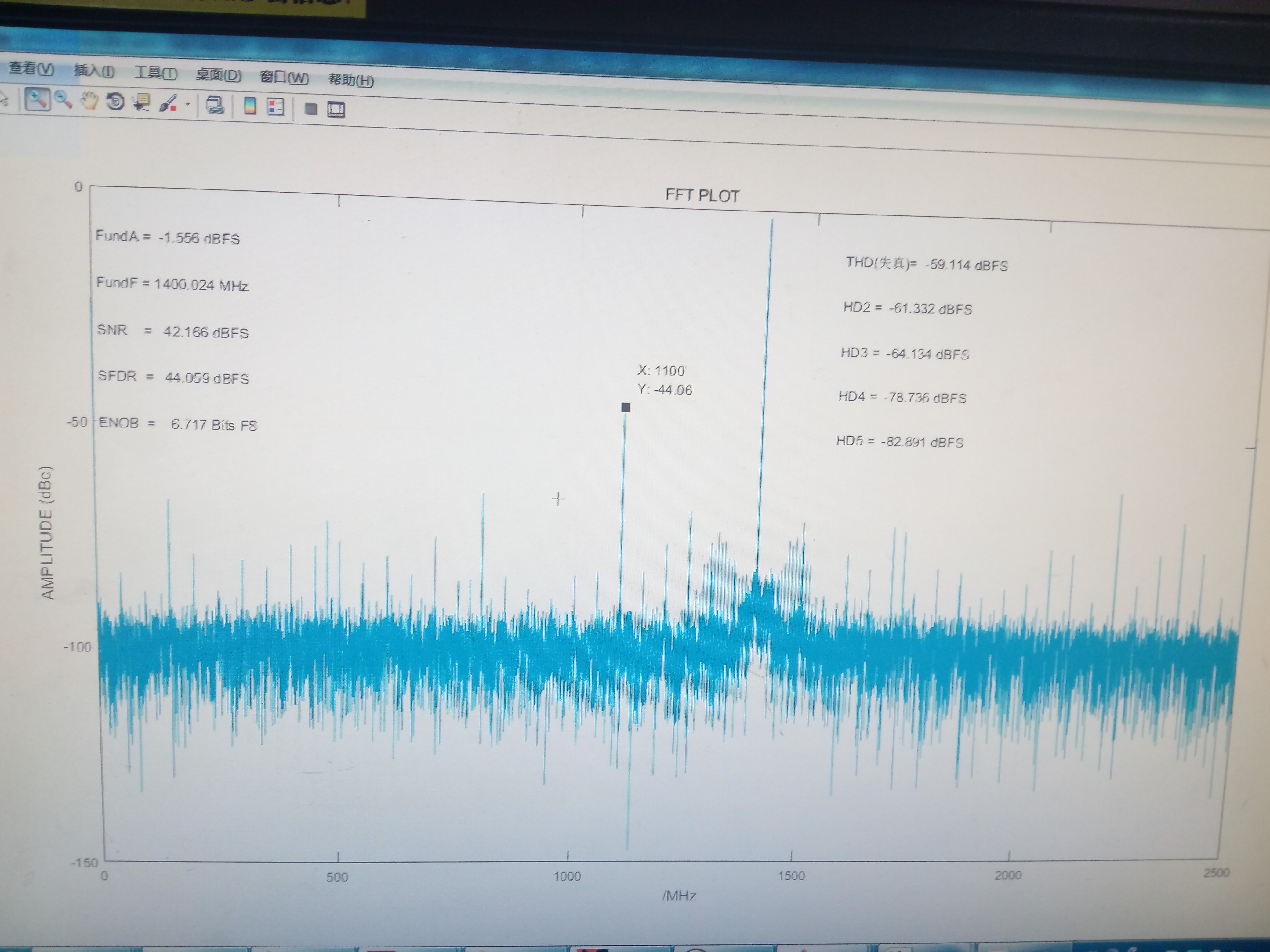
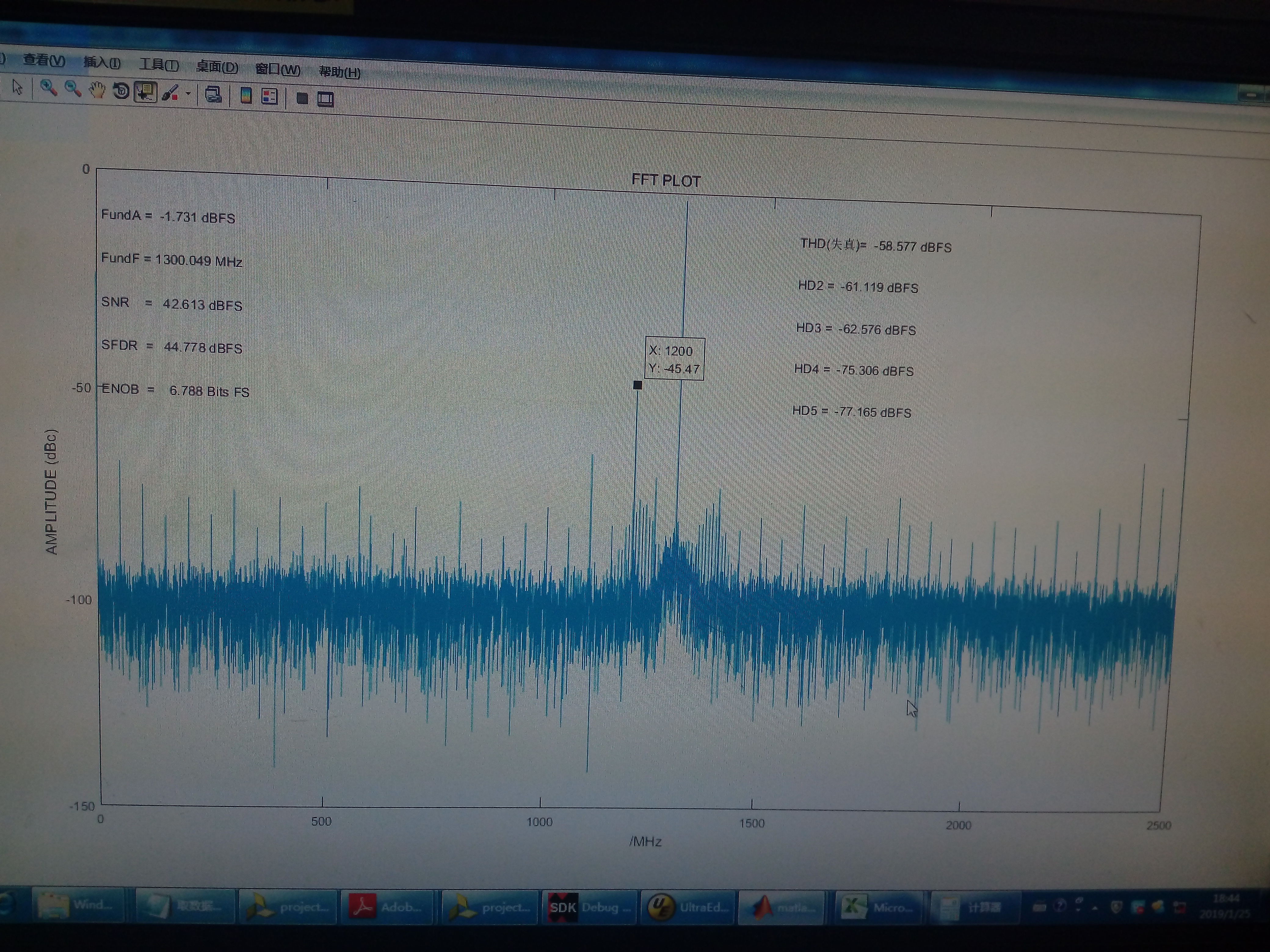
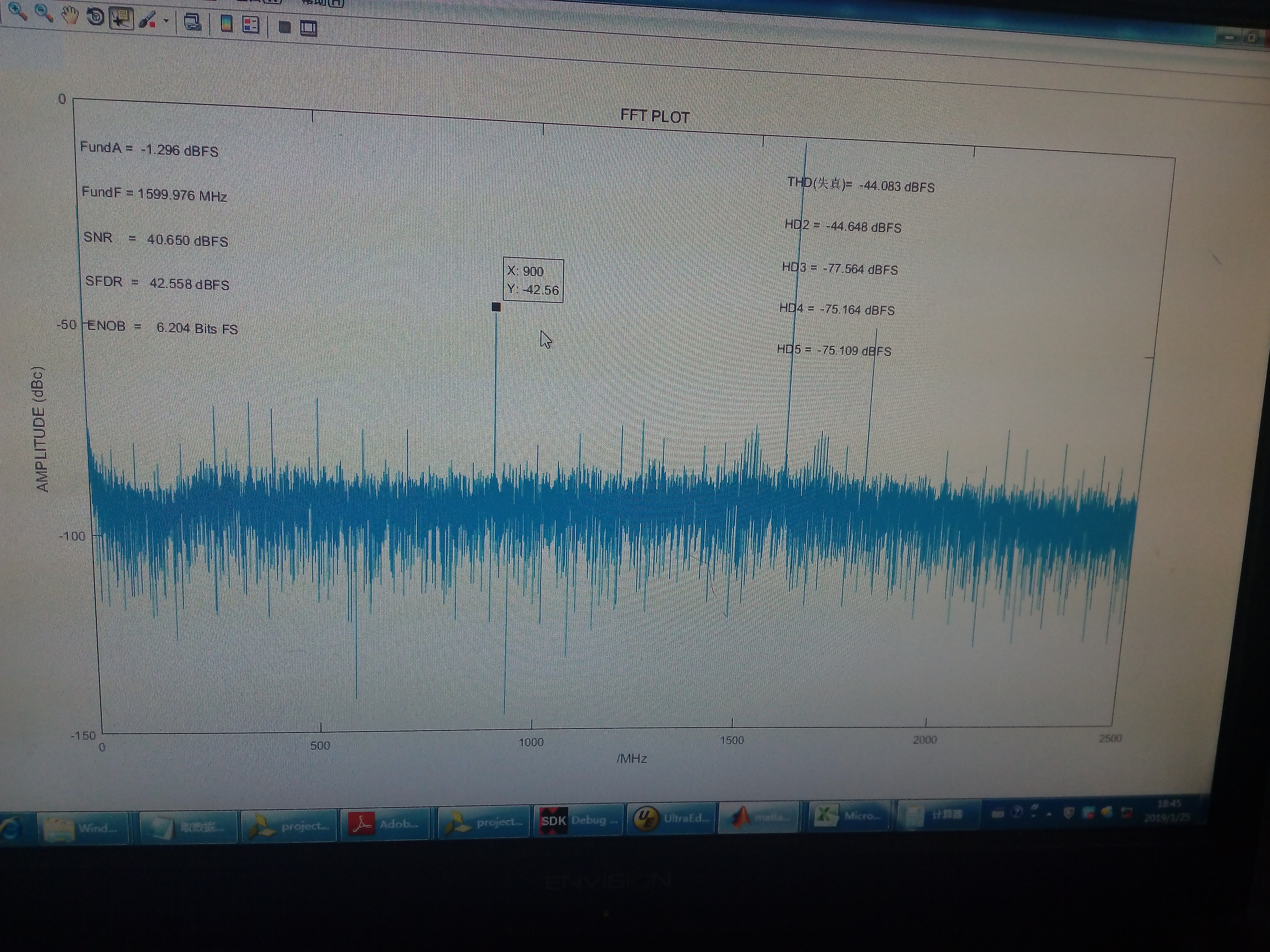
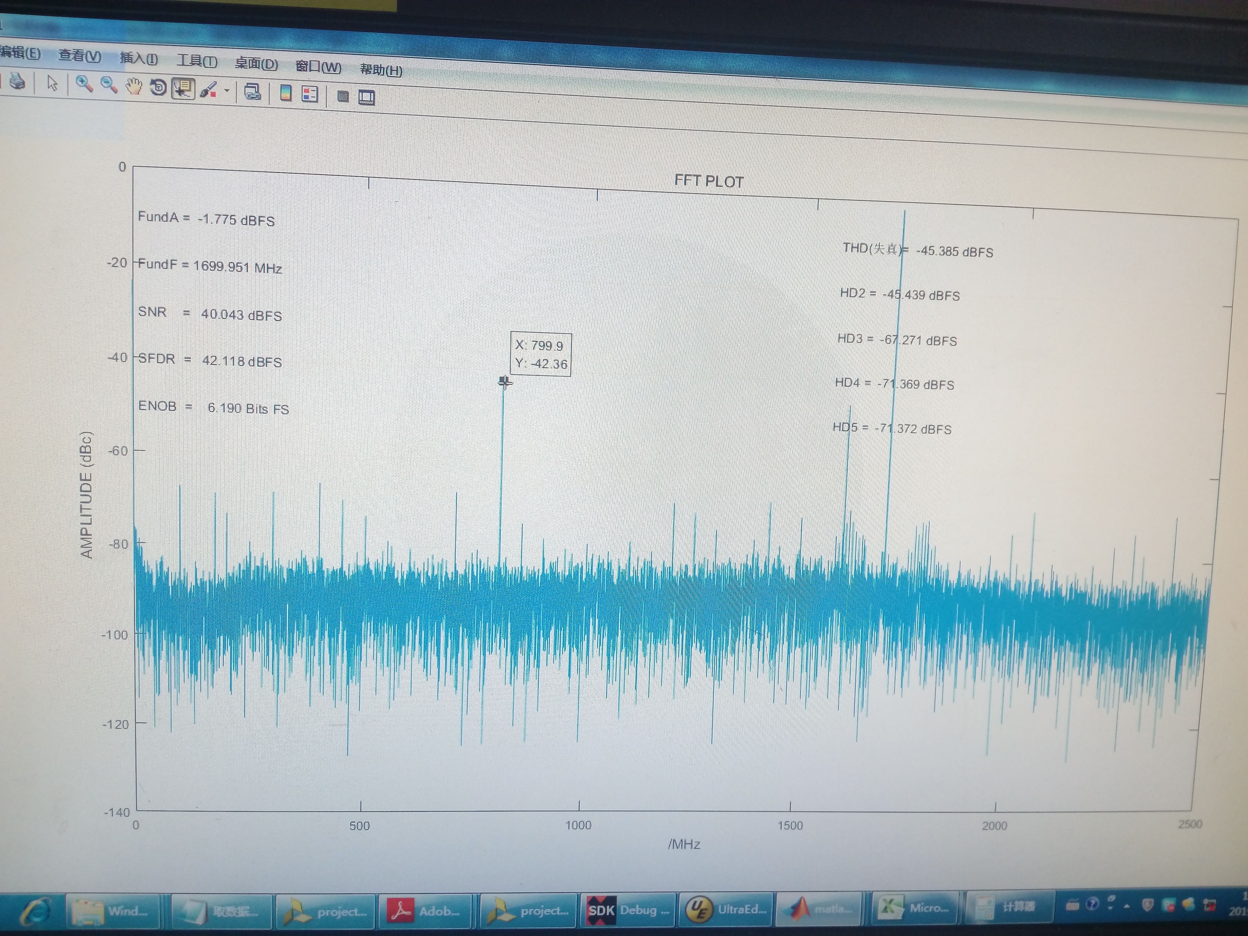
After the analog-to-digital convertion and spectrum analysing via matlab program, we found that the spur at Fs/2-Fin is too high in magnitude and worsened the SFDR performance(perhaps also worsened the SNR performance).
So, what may cause the problem? And how can we solve the problem or where to improve the SFDR and SNR performance?
Looking forward to your reply and many thanks!
P.S. the analysed spectrums are as follow:
Fs=5GSPS in Single-Channel Mode, 1st NZ, Fin=1.4GHz:
Fs=5GSPS in Single-Channel Mode, 1st NZ, Fin=1.3GHz:
Fs=5GSPS in Single-Channel Mode, 1st NZ, Fin=1.6GHz:
Fs=5GSPS in Single-Channel Mode, 1st NZ, Fin=1.1GHz:
And, the register configuration of ADC12DJ3200 is as follow:
u32 AD12DJ_REG_BUFFER[AD12DJ_REG_BUFFER_SIZE]=
{
/////*
0x020000, ////// clear JESD_EN,make sure again
0x006100, ///Always clear JESD_EN before clearing CAL_EN,
0x0000B0,///reset
0x000030,///
0x000200,
0x001000,
0x002300,
0x002920, //SYSREF
0x002960, //SYSREF
0x002A02,// 0x002A06, //CLK_CTRL1
0x0030FF,
0x0031FF, //FS_RANGE A
0x0032FF,
0x0033FF, //FS_RANGE B
0x003801, ////0x003800, ////VA11 is used as reference
0x003B00, ///clear TMSTP_CTRL bipolar OR COMS
0x004800, ////Sets the pre-emphasis for the serial lanes to compensate
0x006001, ////INPUT_MUX
0x006201, ///CAL_CFG0 --CAL_OSFILT //////////Calibration 0x00620A //////0x00620B
0x006B00,
0x007000, ////CAL_DATA_EN
0x007100, /////CAL_DATA
0x007A00,/////GAIN_TRIM_A
0x007B00, ////GAIN_TRIM_B
0x007C00, ////BG_TRIM
0x007E00, ////RTRIM_A
0x007F00, ////RTRIM_B
0x008000, ////Adjust for A-ADC, Single Channel ,Foreground,TADJ_A_FG90
0x008100, ///Adjust for B-ADC, Single Channel ,Foreground,TADJ_B_FG0
0x008200, ///Adjust for A-ADC, Single Channel Mode, Background ,TADJ_A_BG90 ///0x008280,
0x008300, //Adjust for C-ADC, Single Channel Mode, Background,TADJ_C_BG0
0x008400, ////Adjust for C-ADC, Single Channel Mode, Background,TADJ_C_BG90 ///0x008480,
0x008500, ///Adjust for B-ADC, Single Channel Mode, Background, TADJ_B_BG0
0x008600, ///Timing Adjust for A-ADC, Dual Channel
0x008700, ////Adjust for C-ADC acting for A-ADC, Dual Channel
0x008800, ////Adjust for C-ADC acting for B-ADC, Dual Channel
0x008900, ///Adjust for B-ADC, Dual Channel
0x008AFF,
0x008B09, ////Adjustment for A-ADC and INA,when ADC0 samples INA
0x008CFF,
0x008D09,////Adjustment for A-ADC and INB,when ADC0 samples INB.
0x008EFF,
0x008F09, ////Adjustment for C-ADC and INA,when ADC1 samples INA
0x0090FF,
0x009109, /////Adjustment for C-ADC and INB, when ADC1 samples INB
0x0092FF,
0x009309, ////Adjustment for B-ADC and INA,when ADC2 samples INA
0x0094FF,
0x009509, ////Adjustment for B-ADC and INB,when ADC2 samples INB
0x009700, //////DC_RESTORE
0x009833, ////IIR filter bandwidth--IIR soak time///////Calibration
0x010280, ///Timing Adjustment for Bank 0 (0° Clock)/////Timing Adjustment
0x010380, ////Timing Adjustment for Bank 0 (-90° Clock)
0x011280, ////Bank 1 (0° Clock)
0x011380, /////Bank 1 (-90° Clock)
0x012280, ////Bank 2
0x012380,
0x013280, ////Bank 3
0x013380,
0x014280,////Bank 4
0x014380,
0x015280, ////Bank 5
0x015380, ////Timing Adjustment
0x016000, ////LSB Control
0x020101, ////JMODE3---3/////JMODE1-----1
0x020203,///K is the number of frames per multiframe
0x020301, ////
0x020400, ////SFORMAT,,bit1,0: Offset binary,1: Signed 2’s complement,,bit0: Scrambler enable/disable
0x020500, ///JTEST,0: normal, 4: Ramp test mode, 5: Transport Layer test mode; 6: D21.5 test mode 7: K28.5 test mode
0x020600,
0x020700, ///When using a JESD204B receiver, always use FCHAR=0.
0x020800,
0x020900,
0x020AFF, ////extra Link A
0x020BFF, ///extra Link B
0x021000, ////DDC Configuration
0x0211F2,
0x0212AB,
0x021300,
0x021400,
0x021500,
0x021602,
0x021700,
0x021800,
0x021902,
0x022000,
0x022100,
0x022200,
0x0223C0,/////NCO Frequency (DDC A Preset 0)
0x022400,
0x022500,/////NCO Phase
0x022800,
0x022900,
0x022A00,
0x022BC0, //////NCO Frequency (DDC A Preset 1)
0x022C00,
0x022D00,//////////NCO Phase
0x023000,
0x023100,
0x023200,
0x0233C0, ////NCO Frequency (DDC A Preset 2)
0x023400,
0x023500, ////NCO Phase
0x023800,
0x023900,
0x023A00,
0x023BC0,/////NCO Frequency (DDC A Preset 3)
0x023C00,
0x023D00, ///NCO Phase
0x024000,
0x024100,
0x024200,
0x0243C0,////NCO Frequency (DDC B Preset 0)
0x024400,
0x024500, //////NCO Phase
0x024800,
0x024900,
0x024A00,
0x024BC0, /////NCO Frequency (DDC B Preset 1)
0x024C00,
0x024D00, ////////NCO Phase
0x025000,
0x025100,
0x025200,
0x0253C0, /////NCO Frequency (DDC B Preset 2)
0x025400,
0x025500, ////////NCO Phase
0x025800,
0x025900,
0x025A00,
0x025BC0, /////NCO Frequency (DDC B Preset 3)
0x025C00,
0x025D00 //////NCO Phase----//DDC--- NCO Phase
//////*/
};
u32 AD12DJ_REG0[AD12DJ_REG0_SIZE]=
{
0x02B000,
0x02B105,
0x02B001 ///SYSREF Calibration ,,Ensure that ADC calibration is not currently running before setting SRC_EN
};
u32 AD12DJ_REG1[AD12DJ_REG1_SIZE]=
{
////////////READ 0x2B2~2B4 before next
0x02B500,
0x02B600, ///DEVCLK aperture delay adjustment
0x02B700,////Invert DEVCLK by setting this bit equal to 1
0x02C11F,///ALM_STATUS
0x02C21F,////ALM_MASK
0x006101, ///Always set CAL_EN before set JESD_EN
0x020001, ////// set JESD_EN
0x006C00,
0x006C01 /////CAL_SOFT_TRIG
///*/
}

