This thread has been locked.

If you have a related question, please click the "Ask a related question" button in the top right corner. The newly created question will be automatically linked to this question.

ADS8689: Writing to configuration register does not reflect changes

Part Number: ADS8689

I am using ADS8689. I am getting ADS conversion results successfully from the converter with default settings. Now I want to change range of the AD converter. But when I try to write the register, it does not change the range. I have tried lot of combination to write 32bit command word. But I am not getting success.

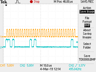
code snippet is below. Clock is given using bit banging

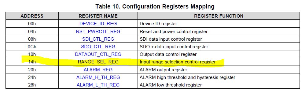
uint32_t BitMask = 0x80000000, Command = 0xD0140002;
 uint8_t ClkCntr = 0;

//select the ADC
 CLRPIN(0, SPI1_CS1);
 SmallDelay(CLOCK_DELAY);
 while(ClkCntr < 32)
 {
  // put data
  if(BitMask & Command){
   SETPIN(0, SPI1_MOSI);
  }
  else{
   CLRPIN(0, SPI1_MOSI);
  }
  SmallDelay(CLOCK_DELAY);
  // Data latched on rising edge
  SETPIN(0, SPI1_SCK);
  SmallDelay(CLOCK_DELAY);
  CLRPIN(0, SPI1_SCK);
  BitMask = BitMask >> 1;
  ClkCntr++;
 }
 // Command processing starts
 SETPIN(0, SPI1_CS1);
  • Hello,

    We highly discourage using bit banging to provide the clock. Although it might work for evaluation purposes we do not recommond this for long term solutions. When you configure the input range, what resoluts are you seeing? is the input range changing, but to the incorrect range? or is there no effect at all?

    Seeing how you are already communicating to the device correctly to output the convesion results in default mode, it sounds as t is not a timing issue. Regardless I would suggest connecting the digital lines to a scope, this will provide a visual of the input data and can be compared to what you are expecting it to be.

    The register to change the input range is the RANGE_SEL_REG. I would suggest, for debugging purposes to only configure one register at a time. Once that is successful, then configuring multple in one command. this means focusing on the 0-3 bit of the command, as shown in the second imege below. When testing, use a DC known input value, this way you will know the expected output.

    Regards

    Cynthia

  • Hi Cynthia,

    Thank you for the reply.

    When I try to change the range, I am not seeing it change at all. It is working with default setting only, which is -12.288V to +12.288V. I am using 5VDC input to ADC for testing purpose.

    I understand that bit banging has some issues. I will change it later when the driver is integrated with our final product code. For now, I am using bit banging in a hope to resolve the issue.

    I have attached screenshot of waveforms of clock with MOSI signal. I have ensured that the timings are being followed with sufficient allowance.

    Some more doubts I have are

    1. Is my command word correct? I am using 0xD0140002

    2. I assume that bit will be latched in ADC on rising edge of clock. Is it correct?

    3. Can I change range anytime after power on?

    4. Is there any particular command sequence to be followed? or I can simply send 32bit command word and continue to read conversion results as usual?

    Please look into issue and do reply to me. I need to resolve this issue.

    Thank you. 

  • Hi Shaziya,
    Cynthia is out this week. The answers to your questions:
    1. This command is correct if +/-1.5Vref range is expected.
    2. The ADC supports SPI-00-S protocol for data read and write operations on power-up or after coming out of any asynchronous reset. The capture edge is Rising of SCLK.
    3. Yes.
    4. Can you please read the register with 0x48140000 command? since the write command gets executed at the rising edge of next CONVST/CS signal, also the eight bits of register content will be returned in the next frame, hence three frames are needed. Please capture the screenshots of waveforms for SCLK,MOSI,MISO and CONVST/CS together.


    Thanks&regards
    Dale

  • Hi Dale,

    Thank you for the inputs. Please help me with some more queries.

    I tried reading back the register contents. I am getting 0x7F in first 8 bits if only 8 clocks are applied for reading. Should I always apply 32 clocks or I can only apply as many clocks as required.

    When 32 clocks are applied, should I consider most significant bits or least significant bits. Is there any thumb rule for this.

    When I am reading ADC conversion results, I am applying only 16 clocks. That means, I am taking 16 most significant bits from ADC. But for reading register contents, this seems to be failing somewhere because I am not getting expected contents.

    I checked waveforms on digital storage scope. It seems to be correct. Rise and fall times are sharp hence delays may not be issue.

    For your information, I am using 5V supply for both digital as well as analog power of ADC. The digital signals from processor are made TTL compatible through level shifter.

    regards

    Shaziya

  • Hi Shaziya,

    The host controller can use a short data transfer frame to read only the required number of MSB bits from the 32-bit output data word, as explained in the Data Transfer Frame section. Please note that the command frame is 32-bit, and also the device sends content of register in the next frame. Can you please explain what command you are using to read the register? Also, please upload the timing plot of the command frame and next frame you got.

    Thanks&regards

    Dale

  • Hi Shaziya,
    I did not get your response, this query will be closed. Please let me know if you have further question.

    Thanks&regards,
    Dale