This thread has been locked.

If you have a related question, please click the "Ask a related question" button in the top right corner. The newly created question will be automatically linked to this question.

DAC7821: Max output coming is 9.97V not 10V

Part Number: DAC7821

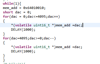
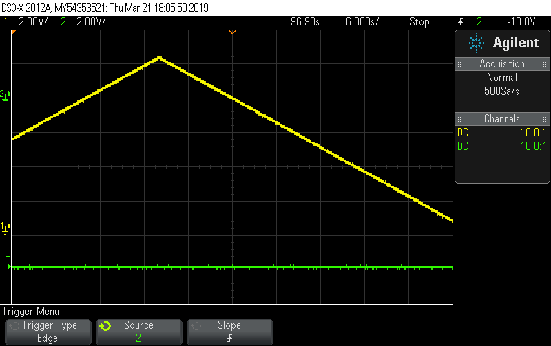
Hello everybody. I am using DAC7821 which is a 12 bit parallel DAC which is interfaced to Infineon XMC4800 microcontroller. I am using it as unipolar output of the range 0V to 10V. If I write the DAC code to DAC data register output is coming correctly. But if I write (9.98*409.6) to the register out put is zero. So the maximum output is 9.97.

But as per my understanding the maximum digital input you can given to the DAC is 111111111111 which corresponds to FFF. But in my case If I give 9.98 the corresponding digital code bit will be 111111110111 which comes below the maximum range. Am I understood it correct?? 

  • Vinay,

    I am not sure I understand exactly what the issue is, but I will try to give an explanation.

    For any DAC device the LSB size is calculated as VREF/(2^bits). In this case assuming a 10V reference the LSB size would be ~2.4414mV. The full-scale value for the DAC is 0xFFF, which means the maximum output would effectively be 4095*2.4414mV = ~9.9975V. The datasheet also specifies full-sale gain error of +/-5mV typical and +/-10mV maximum, so it is possible for the full-scale voltage to be as low as 9.9875V.

    This is an unbuffered R-2R DAC, so most likely your setup also includes an output buffer which could contribute additional errors.

    The reference is probably not exactly 10V, which is maybe contributing more errors.

    Maybe you can share the more complete system view for us to evaluate if 9.97V full-scale output is reasonable.
  • Hi Kevin,

    Thank You for your response. I have attached schematic for your reference.

    I was trying to generate triangular waveform by writing values from 0 to 4095 to DAC register. But at some points, the voltage is suddenly dropping to zero. I have checked the triangular waveform with respect to chip select signal and RW signal. But I could not get any inference because that dip in voltage is very random. I have attached scope images for the reference.

    Below is the schematic

    below is the scope of triangular waveform

    Below is the zoomed scope

    Below is the code for DAC

    Thank You

  • Vinay,

    Is it possible for you to trigger your oscilloscope on one of these falling edges of the output waveform while monitoring the RW/CS/Data timing? Just at the surface level this doesn't seem like an analog problem, it would appear to be some marginal timing which is randomly manifesting itself as these output glitches. If this isn't possible maybe a worthwhile experiment could be simply slowing the master clock for the host controller to relax all of the timing, and checking if this artifact goes away or not.

    What is going on with the OP282 and ADR01 circuit? Having a hard time seeing how that feedack loop is closed, though I did not spend a significant amount of time with the ADR01 datasheet.
  • Vinay,

    Do you have any update on this topic?
  • Hi Kevin,

    Thank you for your response.

    1. Actually, now output is coming correctly. Even spike is also not coming on triangular waveform. There was a issue with chip select signal timing. Before it was like, the amount of low time of chipselect signal was greater than amount of low time of Write signal. I reduced the amount of low time of chipselect signal to the time of Write signal. Issue got solved. The data will be latched to DAC register at the positive edge of chipselect signal. But in our microcontroller(XMC4800), the data will be available even after WR signal goes high. So when chip select signal is low even after WR signal goes high proper data will be available on data bus. But output is not coming for this case. Spikes will come on certain points.

    2. If I introduce a delay of certain milliseconds while incrementing every bit (0 to 4095), on triangular waveform I should be able to see step like behaviour. For the amount of time the delay is introduced same voltage has to come. But I did not observe steps. What could be the cause for this?

    Thank You

  • Vinay,

    Unfortunately I do not really follow the commentary or question for item 2. Could you elaborate further?
  • Hi Kevin,

    Thank You for your response.

    1. In the first statement my question was, if low time chip select signal is greater than low time of WR signal will I get output? See in the below figure time t1 is the time between positive edge of WR signal and CE signal. For this case, voltage will drop to zero for certain point (certain DAC code). On the triangular waveform there will be spikes (see the waveform attached in previous post)

    If I make t1 is zero which means positive edge of WR and CE occurs at the same time then it works fine. My question is at time t1 data on the data line will be vallied data based on the microcontroller that we are using. But still output drops to zero for certain DAC code.

    2. In second statement my question was, If I don't give any considerable amount of delay while given data from 0 to 4095 to DAC in a for loop, the Vout  waveform should look like below.

    Here minimum point corresponds to 0V and maximum point corresponds to 9.997V.

    But I introduce certain milliseconds of delay in for loop while incrementing every bit from 0 to 4095

    ex

     *(uint16_t *) ptr  = (409.6 * 0);

    Delay(500); //ms

     *(uint16_t *) ptr  = (409.6 *1);

    Delay(500); //ms

    .

    .

    .

    so on upto 4095

    For this the Vout waveform should look like below

    Here based on the amount of delay that you have given the output should remain same at the same level. But I am not observing this in my waveform. The waveform is coming like the one with no delay. Even I tried to zoom it to maximum on CRO by increasing the time division.

      In our project we have given output of DAC to a VFD(Variable frequency drive) which in turn runs a motor. So at a time time we can't give 0 to  maximum input because it takes time to accelerate. So we need to give certain amount of delay in between while writing to DAC.

    Thank You

  • Vinay,

    The status of the R/!W pin needs to maintained for the full duration of a read or write cycle with respect to chip select. So, for a write sequence the pin needs to be kept low until a rising edge on CS. They may rise at the same time, but R/!W cannot rise before CS for a valid write cycle. This is captured in timing parameter t2 in the datasheet - indicating that the minimum time from a CS rising edge to R/!W rising edge is 0ns - as opposed to "negative time" allowing for R/!W to rise before CS.

    Concerning the second item, where in your schematic are you measuring the output? OUTA_P? Is there anything else connected to this net?
  • Hi Kevin,

    Thank You for your response.
    Yes. We are measuring output at OUT_P. As of now, for testing purpose we have not connected any load to output. So nothing is connected at the output.

    If I increment one bit every time 2.44mV will be increased. If I increment 4 bits at a time 9.76mV (~10mV) will be increased at the output. In order to see the clear step waveform I will increment 4 bits at time and after reaching 4095 I will decrement 4 bits till it reaches 0 in the for loop. I will establish delay of 100ms in between each increment. On CRO I will set time division as 100ms (X -axis) per division and Voltage division as 10mV per division (Y- axis). For this kind of setup, I should be able to see a clear step for each horizontal and vertical division of CRO right? But I am not able to see this.
     
    Thank You

  • Vinay,

    Can you share the oscilloscope capture of the output response? Along the way, having the reference in the same capture would be helpful.
  • Hi Kevin,

    Thank you for your response.

    I have attached oscilloscope capture of output response along with reference voltage. I have given the delay of 50ms and every time I incremented 4 bits which corresponds to almost 10mV. But on the oscilloscope I have kept the time division as 6.8s per division and voltage as 2V per division. When I set the division as 50ms per division and 10mV/div then I could not capture the whole graph as it is not possible. Can you reproduce the setup as I told in the previous post at your lab? If so can you send me the output response?


    Thank You

  • Vinay,

    Unfortunately DAC7821 does not have an EVM and is a bit on the old side - so I do not have any hardware readily available in the lab to do any testing. The best case would be ordering a DIP adaptor board and some sample units to try to put something together, but it is going to have some parasitics which may corrupt the measurements. I can see what we can do.

    Meanwhile, can you zoom in more on the ramp waveform? From this resolution the output steps appear to be visible, so I'm still sort of struggling to see what the real remaining problem is.
  • Vinay,

    I've been out of office on business travel this week, but I thought I would check back in on if you can get a chance to zoom in on the previous capture.
  • Hi Kevin,

    Sorry for the late reply. I was on leave so I could not reply. if I zoom the previous waveform the steps could be visible. I think that much is acceptable. Thank you for your support.

    Regards
    Vinay
  • Vinay,

    That is great news! Please let us know if you need any further support at all.