This thread has been locked.

If you have a related question, please click the "Ask a related question" button in the top right corner. The newly created question will be automatically linked to this question.

Linux/ADS7841: ADS7841

Part Number: ADS7841

Tool/software: Linux

Hello,

I am trying to measure the voltage at channel 0

CMD 0x97 represent below configuration.

7  Bit      =>   Start Bit. Control byte starts with first HIGH bit - 1b
6-4  Bit   =>   A2 - A0 Channel Select Bits - 001b (channel 0)
3 Bit       =>   Mode - 0b (12Bit ADC)
2 Bit       =>   Single-Ended Channel Selection  - 1b
1-0Bit    =>   Power-Down Mode No power down- 11b

I am observing random values at MISO line. Could you please review the command value. Is there any test mode/command available to check validate the ADC chip response.

From  your previous comments,

>>how many clocks per conversion are you sending?

How can I check the configured clock per conversion?

  • Hello,

    What are you seeing at the MISO line? Is the measurement showing the result of a different channel, is there a pattern?

    The command you are using seems correct. In the orignal post, it seems you were able to achieve correct measurements, the difference I see is that you are trying to make is from 8 bit to 12 bit, is this correct? To do so, the MODE BIT needs to be changed from high (8 bits) to low (12 bits). Side note, the MODE PIN needs to be tied HIGH for the configuration to take place. If the MODE PIN is pulled low, the device will always be set for 12 bits.

    I would suggest connecting the digital lines, MISO, MOSI, SCLK, and CS to a scope prob, this will make it easier to debug as you will be able to visually confirm that the MOSI line is showing what is expected, and confirm the digital communication. Use known DC values at the input, to confirm the output measurement.

    In the precious post, he was asking how  many clock pulses are being sent to the device per conversion. This device has multiple options, 24 clocks, 16 clocks, or 15 clocks. This depends on the user.  The most common is 16 clock per conversion, see image below.

    Regards, Cynthia

  • HI,

    Thank you for your comments.

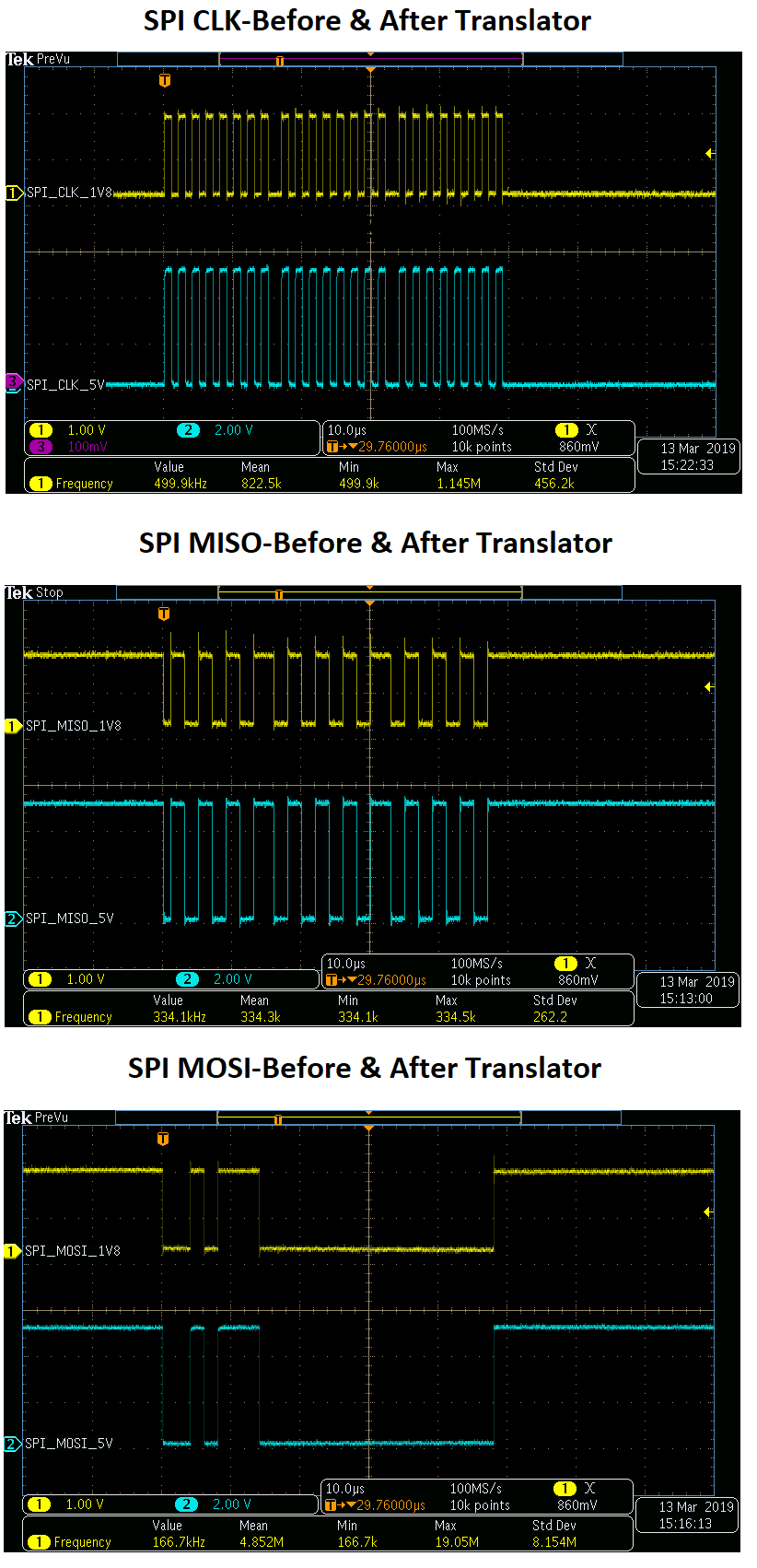
    There is voltage level shifter in between CPU and ADC chip.MODE pin is low in my hardware.

    By seeing the sequence diagram, I feel I need to configure my master-SPI controller with LSB first option and the ADC chip in MSB first configuration.
    Is that correct?

    I could see the sending in MOSI line but random data in MISO line .

    This behaviour is same for 12Bit and 8Bit and converted value doesn't match to the giving voltage to the channel.

    I am attaching one probe instance for your reference.

    Is there any test mode for this ADC chip so that I can expect a pre defined pattern in the MISO line?

  • Hello,

    If in your hardware, Mode pin is pulled low, then you wil not be able to use 8 bit conversion. You will only be able to use 12 bit conversions, even if you change the command. The hardware will overide it.
    Both the Master and the ADC should be set to MSB first configuration.

    The first bit of starting a new conversion command needs to be High, this is the start bit. If this bite is not set, then the device does not recognize the command you are sending it. Taking a look at the MOSI (SDI) line it seems that you are not setting this bite high, thus the device will not performace the commands expected.
    The digital input to select channel 0, single ended, without powerdown look like: 10010111
    Try giving this command, and let me know what you see on your SDO

    Regards,
    Cynthia
  • Hello,

    Thank you for your response. 

    I have few confusions from your replies

    >>The first bit of starting a new conversion command needs to be High, this is the start bit.
    >>The digital input to select channel 0, single ended, without powerdown look like: 10010111

    I Understand that the command which should I use is (MSB)1001 0111(LSB) ie x097.

    >>Both the Master and the ADC should be set to MSB first configuration.

    1. Based on this comments, SDI line should be contains data in below sequence of bits.
        (LSB)1110 1001(MSB).In sequence ,the Start bit is High as per the ADC chip requirement. Could you please comment.

    2. After 0x97 command, 2 set of 1byte (0x00) dummy data to get the 12bit of ADC data from the chip.

       Is that approach is proper?

    3. To calculate the voltage, I am taking the last 12 bit of data.The calculation mentioned below.

        12bit data for 1 test instance

        data  = 1000 0000 0000b which is in decimal 2048

        Bit factor  = 5/2^12 = 5/4096 = 0.00122. (Revfence voltage is 5V and 12 bit ADC mode  )

        Voltage w.r.to observed data = 2048x0.00122 = 2.49V

        Is the calculation method proper?

    4.The Channel 0 in the attached image is for BUSY Line from the ADC chip.I could see some difference when I am comparing with conversion timing diagram.After the command, BUSY line should go low and user need to consider the converted data when the BUSY line is low.But I could see data in that time. The given attachment is the example.
    Could you please comment on the BUSY line behaviour .Is that expected?

    Attaching SPI lines behaviour for your reference.


  • Hi ,

    I have some more experiments corrected the command which I have sending to ADC chip.

    After the command update, I will be considering the 12bits of data after the busy falling down and using the data for calculation.

    It results proper voltage. I am attaching the signal analysis screen shot for your reference.

    I understand that we need to consider the data once the BUSY line goes low.In my experiments, the busy line is going low after 1 clock cycle.
    ie 9th clock data can be skipped and next coming data(12bits of data) need to be considered for voltage calculation.

    Is that expected behaviour? Can I move forward with that concept?
     

    Please note that currently, The BUSY line is not connected to my CPU. So that I am not able to monitor the BUSY line in my application code. 

  • It looks like you are moving in the correct direction

    The command you sent, the first 8 bits are correct to start a conversion sampling channel 0.

    When Busy is high, you should not be clocking out data, there can be slight overlay, which can be seen in the timing diagram, but you need to make sure the 9th clock data is not skipped.  I would suggest monitoring the BUSY signal to make sure that timing errors do not occur nor SDO data is skipped.

    You mentioned that you send a 16 clock pulses as dummies clock out the data, this approach works. If you use the device with 16 clock cycle per conversion, you can also send a command on SDI on the second byte (second set of 8 bits) to the device to sample the next desired device. Take the image below as an example.

    You are calculating the voltage measurement from the SDO data correctly

    Regards, Cynthia

  • Hello,

    Thank you for your response.

    >>You mentioned that you send a 16 clock pulses as dummies clock out the data, this approach works.

    Okay,I will follow this approach for getting the ADC data from the chip.

    Here,my concern is BUSY line is not connected to CPU.So it may not possible to monitor the line.
    As I mentioned in previous post, after 9th clock cycle only the BUSY line going low.So can I consider that approach to take the ADC values?

  • It would be best to monitor the BUSY line, but if you cannot, then using other timing schemes will need to be implemented.
    If you have seen that using the 9th clock cycle as an indicator has been correctly working, then it is fine to continue doing so.

    Note that if you change the device timing, such as sampling rate, the busy time may be affected, and you will need to make sure again the 9th clock cycle provides enough time for BUSY to go low.
  • Hello,

    Thank you for your response.

    I will be going with 9th clock cycle as indicator for ADC method.

    I would like to know the BUSY line monitoring based ADC data read mechanism concept. So that we can use the same for next revision board with busy line support.
    Here my confusion is SPI read is synchronous with CLK. in that case how can I identify the data which is at low BUSY line. Could you please give some comments

  • Sure, BUSY indicates when the device is making the analog measurment, so it is best there there is no movement within the device during this time, such as clocking.
    You can use BUSY to monitor when the device is in this state and use the falling edge of BUSY as an indicator to start clocking out data. For the ADS7841, the SDO data after BUSY goes low is the measurement data of the channel that was asked for in the control bit command.
    This can be different in other devices with internal registers, or are simultanous sampling.
    Regards,
    Cynthia
  • Hello,

    Thank you for your response.

    Here my understanding is mentioned below from your response.

    1.Send the 8bit command.
    2.Monitor the BUSY line for falling edge
    3.Send 2 set of 8 bits dummy data to get the data from ADC chip if the after getting the BUSY line falling edge condition.

    Is the understanding correct?

  • Correct, your understanding is correct
  • Hi,

    Thank yo for your response.

    I would like to discuss ADC chip response observation.

    I am getting the proper values after the consecutive sending of ADC command.
    Example, if I am sending the command 1 time(first time) , the expected values are not coming.(expected value means the ADC values for given input voltage).

    If I am resending the command for 20 or 10 times, then I will get the proper. So I am planning to take 50 samples to calculate the input voltage.

    Is that expected behaviour? Is chip required time to get stabilise to output the values or user need to send commands repeatedly to get the ADC values..?
  • Hello,
    Does this only happen during the first conversion after start? or does it happen periodically as you run the device?
    Is the data completely wrong, or random, or does it look like bits are missing? This could be due to clocking data out when BUSY is high, and data from two conversions are being mixed.

    Regards
    Cynthia
  • Hi,

    Mainly it is happening for 1 data after conversion. Currently I am taking 10 samples and processing the average for safer side.

  • Given this is a mux-ed device, it can make sense that the first conversion does not hold valid data. I would suggest ignoring the first conversion. If there are no issues in the rest of the data out, then averaging will also work
  • Hello,

    I am clear now. We can consider that this thread as closed.

    Thank you for your valuable responses and support.

    All the best.