This thread has been locked.

If you have a related question, please click the "Ask a related question" button in the top right corner. The newly created question will be automatically linked to this question.

ADC128D818: Channel Readings Registers LSByte sticks at 0xFF

Part Number: ADC128D818

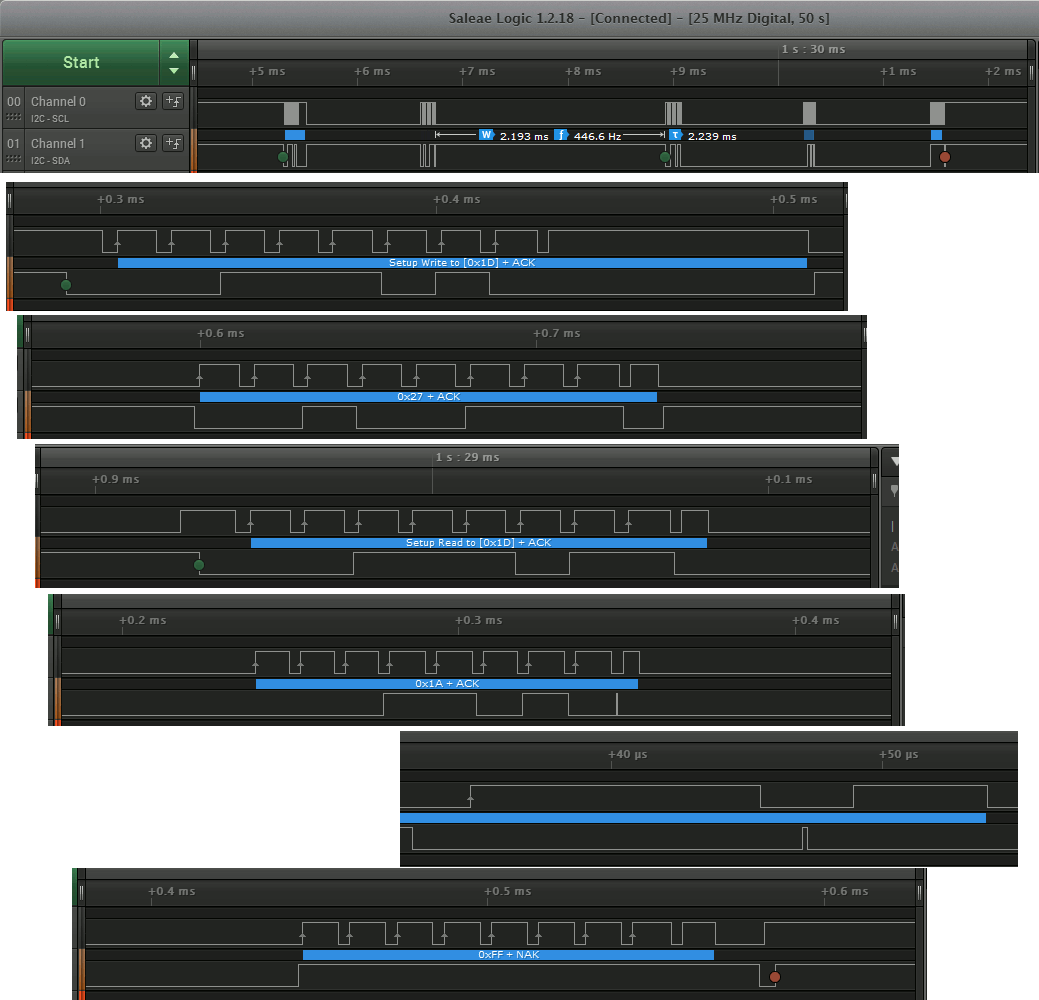
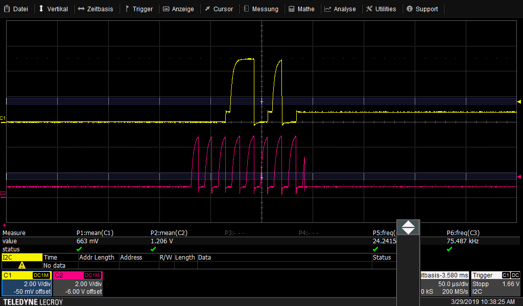
I set up a ADC128D818 to convert continuously in mode 2 (four differential inputs). The MSByte seems to be read correctly, but the LSByte sticks on 0xFF (on all four channels). Is there something I've forgotten, like switching to a 16-bit-mode?

Thanks in advance, Peter

  • Also the Temperature Reading register 0x27 has it's LSByte stuck at 0xFF. Therefore I can read only the integer part of temperature in °C.
  • Forgot to mention: I have observed the I²C telegram by means of a logic analyser, so I rule out that there is a software problem in receiving data
  • Peter,


    Can you post the output of the logic analyzer? It might help to show what I2C communication is formed. I'm not sure what to look for, but maybe there's some sort of stop by the master after the first data byte. At the very minimum we can see if the device has fully acknowledged all the bytes of communications.


    Joseph Wu
  • Thanks for asking, I don't know yet, but maybe the question lead me to a solution.

    In the following there is the view from the logic analyser. At top, one can resemble the total data telegram. Below there is a zoom into each individual byte transmission. The last but one line is view to a SDA glitch where host takes over SDA in order to say "ACK" to ADC128D. This seems to be no problem, as this is a valid I²C signal as long as SCL remains low during the glitch. But this event let me dig further. I connected an oscilloscope and examine this range. See below.

    Note: The oscillograph isn't from the same transmission as the logic analyser view. In fact, it was recorded the next day. Due to isolation involving ADUM1250, one can observe the actual low level and infer from that the signalling direction: A 0.0-V-low comes from device, a 0.6-V-low is from host. Conspicuous are the slurred edges. In fact, the last clock pulse indeed gives a barely squeezed sufficient TTL level, but ADC128 needs a CMOS alike logic level of 0.7·5 V = 3.5 V, which is missed by that wimpy clock pulse. (Note that the top picture is taken by analyser that is connected to the other side (host side) of isolation, where less slurring occurs.)

    I guess that ADC128D misses that clock pulse. When host tries to receive the next byte, supposedly the first then clock pulse will be understood as ACK's clock pulse. As host expects data from device and device expects ACK from host, this yield a NACK, which correctly prompted ADC to release the bus.

    I'll try to improve the signal, either by slowing down transmission or by give stronger pullups on isolated bus segment.

    Thanks for the time being, Peter

  • Now it works!

    Thanks, Peter