This thread has been locked.

If you have a related question, please click the "Ask a related question" button in the top right corner. The newly created question will be automatically linked to this question.

THS1206: Data_AV issue

Part Number: THS1206

Hi Team,

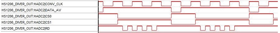
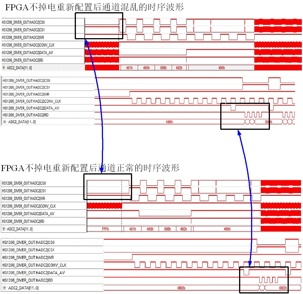
According to the description of DATASHEET, the first RD pulse output after the DATA_AV signal is channel 1, the second RD pulse output channel 2, third RD pulse output channel 3, and fourth RD pulse output channel 4.
Based on above timing control, the RD pulse after the DATA_AV signal does not correspond to the respective channel number.
When the power is initialized, the first RD pulse output channel 4, the second RD pulse output channel 1, and the third RD pulse output channel 2, fourth RD pulse output channel 3.

The data captured on CH1 is output on CH2 while the CH2 data is output on CH3. 

Could you please help to advise how to solve this issue?

Thanks.

  • Hi Johnson,

    Without seeing any timing from the system, the only suggestion that I have at the moment is to go back and review the datasheet again.  The THS1206 is a pipeline converter and there are specific instructions in the datasheet on when to start applying the RD impulse based on the configuration of the device and the FIFO trigger level.  Please provide screen captures of the control lines and we can help you debug this further.

  • Hi Team,

    1: The initial configuration timing of the system is as follows (1st diagram):
    1.1 After power-on, first write RESET reset information to HS1206. H'401
    1.2 Clear reset H'400
    1.3 Write working mode to CR0 H'098
    1.4 Write FIFO reset control signal / CR1 mode configuration H'492
    1.5 Clear FIFO Reset H'490

  • Thank you Johnson,

    Can you get a logic analyzer capture that shows the test bench capture? Please include the initialization sequence up to the first batch of read cycles.
  • Hi Tom,

    Below is the abnormal (top) vs normal (bottom) initialization sequence up comparison. 

    Since the FPGA is uninterrupted power down, and the reconfiguration time is likely to be reconfigured at CS0 = 0 / CS1 = 1, due to the status of CS0 / CS1 may be inconsistent during this initialization.
    However, there is a global reset instruction in the initialization operation, which should not be subjected to the CS0 / CS1 state before the configuration reset influences.

    Could you help to look into this issue?

  • Hi Johnson,

    I sent you a note offline. Why is the timing different in the four writes to the device (4th rising /WR versus CSx)?