This thread has been locked.

If you have a related question, please click the "Ask a related question" button in the top right corner. The newly created question will be automatically linked to this question.

ADS8168: SDO Communication / Timing Issues?

Part Number: ADS8168

Hi there,

I have an ADS8168EVM, which I have tested the functionality of, with a PHI controller.  To make sure it works with my custom host (which is an Adafruit FT232H USB to SPI), I have brought out all the digital signals and hooked them up to the FT232H.

It seems that I am able to send command from this host correctly but I'm have trouble receiving data from the device correctly. I'm just performing basic register read / writes but it seems that the device toggles data on the clock rising edge, even though my mode is set to 00. Data is sent correctly on the rising edge from the host. 

As an example, I write 3 bytes each time.

First time, I write to Register 00h using the write command, the value 0xAA ([0x8, 0x0, 0xAA])

Then I read from this register using the read command as per below ([0x10, 0x0, 0x0])

I should just get 0xAA on the SDO line at this point but I tend to get garbage bits.

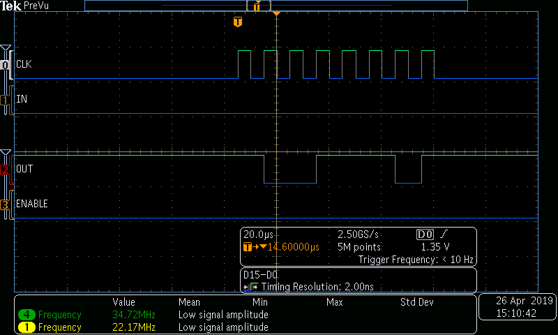
Please see images attached. (IN is MOSI, OUT is MISO)

([0x8, 0x0, 0xAA])

([0x10, 0x0, 0x0])

Read (Data changing on rising edge of clock)

Thank you!

Nik


  • Hi Nik,

    I am not sure I have an explanation in the clock edge discrepancy. However, did you notice that after sending the 24b READ frame, you then retrieve the 8b register data in the next frame?

    This is shown in Figure 57 of the datasheet.

    Regards,
    Keith N.
    Precision ADC Applications
  • Hi Keith,

    Thanks for the response.

    Everytime I do send in the 24b READ frame, I always received random data back on the SDO line. (You can see from last picture)

    In reference to Figure 57, my host doesn't send in 24 clocks one after the other. It sends 8 first and then 16 (both for write and read). Is this an issue? Am I writing data correctly as well, based on my first 2 pictures?

    Best,

    Nik 

  • Hi Nik,

    Based on your first picture, it does appear that you are writing the correct data. There is no minimum SLCK frequency or frame period; should not be an issue writing 8bits, delay, and then the remaining 16bits. The only possible timing issue is the required delay of t-ht_CKCS=7.5nS from the last SLCK falling edge to the rising edge of /CS. (Figure 3) You may be meeting this requirement, but it looks like /CS is going high at the same time as the last falling SLCK edge.

    If the device did not process the WRITE command properly to enable register read back, then you will get conversion data instead of the register contents. This will appear random if the inputs are floating, or if you did not wait for a conversion to complete before taking /CS low.

    If possible, try to capture the above data using a scope instead of a logic analyzer. I am still not sure why it appears that the ADC is launching data on the SDO pin on the clock rising edge.

    Regards,
    Keith
  • Hi Keith,

    Seems that I'm able to meet the t-hkt_CKS of 7.5ns by a large margin:

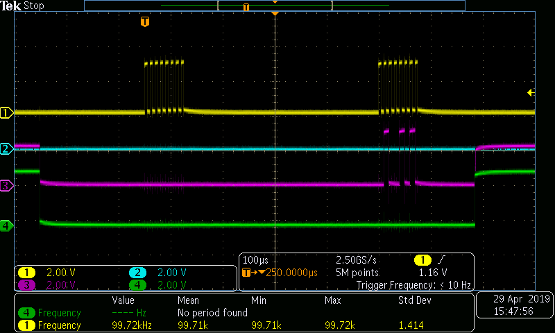
    Here are the same shots but with a scope (  I have also grounded the inputs)

    CH1: CLK

    CH2: MOSI

    CH3: MISO

    CH4: CSB

    Writing 0x8, 0x0, 0xAA

    Writing 0x10, 0x0, 0x0

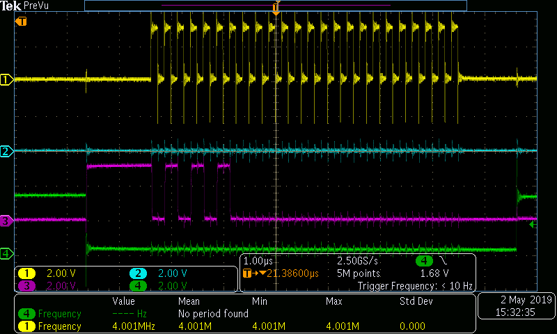
    Trying to read 0xAA

    read 0xAA Zoomed:

    Best,

    Nik

  • Hi Nik,

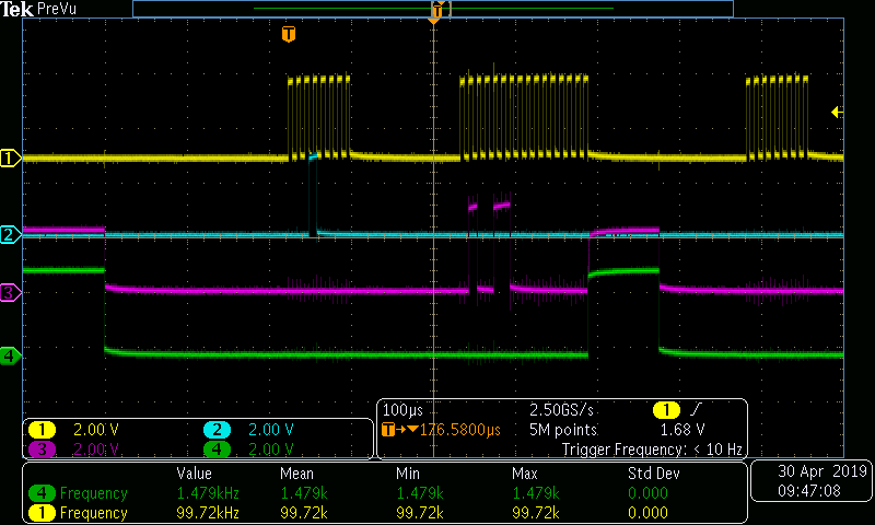
    Can you show the two consecutive frames needed to read from the register in one scope capture (a total of 32 SLCKs)?  

    The first 24b should be the read frame immediately followed by the next data frame (/CS going low for the second time) with at least 8 SCLKs similar to figure 57 in the datasheet.  

    I want to make sure there is no other activity between these two frames which could explain the random data.

    Regards,

    Keith

  • Hi Keith,

    Please see attached. It seems that SDO is "shooting out" some data even before CS goes low again.

    Does this have to do anything with signal integrity or even ground sharing issue? I'm using the ADS8168EVM where I have taken out the PHI controller and soldered 5 wires to my most (SDO, SDI, RST, CLK, CSB). The EVM power is also external using the screw mount (DVDD is 3.3 and AVDD is 5.3V) from a power supply.

    Best,

    Nik

  • Hi Nik,

    The above timing with SCLK looks correct. I think you may be correct that this is a signal integrity issue. You should be able to get this to work, but you may need to slow down the SCLK. Replacing the series resistors on the EVM with 10-50ohm should also help with the edge rates.

    Since you are bringing power into the EVM through the screw terminals, make sure there is a ground wire connected from the EVM board to your HOST board as well. If the HOST is powered from the same DVDD supply, run DVDD and ground wires directly between the HOST and EVM to reduce the path length that the ground currents most flow over.

    Regards,
    Keith
  • Hi Nik,

    The attachment did not make it through. Could you upload the image again, either a *.png or *.jpg will work.

    I suggest doing some basic troubleshooting. Check the AVDD voltage on the ADC pin 32 and verify that it is 5.3V. Check the REFIO pin 3, it should measure 4.096V. When using the external supply connection, I also suggest removing R18 to isolate the on board LDO from the external supply.

    Also, since you are connecting an external host, does this host power from the same supply as DVDD? If not, and it powers up before DVDD on the ADC, it could be causing the device to not reset properly. I suggest making sure the no voltages are present on the ADC input pins until the power supplies are up.

    Since you have external supplies, you may want to force a RESET after the supplies have ramped up to their final value to make sure the ADC is operating in a known reset state.

    Regards,
    Keith
  • Hi Keith,

    I went back to the EVM setup with the PHI controller and it seems that now, even with the GUI, I'm not able to write values to ADC correctly anymore as I used to before. For example, writing 0xAA to register 0xAA through the GUI, the method of write goes through. However, reading back still shows 0x00. It's similar for a lot of other registers.

    Could this have become a faulty EVM?

    Best,

    Nik
  • Hi Keith,

    I have gotten this to partially work. See image below.

    The register content reported back is 0x54 instead of 0xAA. It seems that SDO line is sending out data too early (This on a new part now).

    Screen Image

    Best,

    Nik 

  • Hi Nik,

    With the new part, did you also check proper operation with the PHI board? Unfortunately, I cannot see your screen shot of the data. When you say that the SDO is sending data early, relative to which signal? /CS, SCLK?

    Thanks,
    Keith
  • Hi Keith,

    I have been playing around with some device settings and have gotten this to fully work now.

    I believe there may be some sort of bug with the part. I noticed that upon reset, even on the EVM board with the PHI controller, the ADC SDO changes data on the rising edge which causes the host to the misread the data. This is supposed to be the default SDO Mode 00 with SDO_CNTL1 register set to 0x00.  

    However, the interesting part is, when I change this register setting to 0x01, which according to the datasheet, is an invalid configuration, SDO changes now on the falling edge causing the host to sample correctly now on rising edge, since it's operating in SPI mode 00. 

    Can you please double check this? I'm noticed the same communication issue in the PHI controller as well (SDO changing on rising edge) --> however this works on the EVM because of the sample / hold time is sufficient for PHI controller but the same is not true for my host.

    Please see attached scope shots of my host communication:

    SDO Mode 00 Rising Edge Data Change:

    SDO Mode 01 Falling Edge Data Change (Invalid Config!) but data read correctly from host on rising edge: 

    PHI Controller Read SPI Mode 00, Single SDO, data changing on rising edge but still making it correctly :

    Best,

    Nik 

  • Hi Nik,

    I am glad you got this working on your Host platform. I am out of office this week. I will dig into this further and follow-up later next week once I have a chance to look into this further.

    Regards,
    Keith
  • Hi Nik,

    I confirmed that the ADS8168 launches data on the rising edge of SCLK for SPI-00 mode.  This was done to support a higher speed SCLK frequency.  Most FPGA's and MCU's do not require a hold time after the launch edge, or if they do, it is typically less than 1nS.

    Below is a timing diagram for the SPI-00 mode.  The MSB (D15 in the below example) is launched on the falling edge of /CS.  The host will capture on the first rising edge of SCLK, and this is also the edge that the next bit (D14) is launched.  As long as the digital control signals are clean, this will reliably work.

    In your specific case, since you had jumper wires from your host MCU connected to the ADS8168EVM, you are likely getting ringing that is corrupting the SDO-0 data on the capture edge.  The mode that you selected to launch data on the falling edge of SLCK is not supported and not recommended to use.

    Regards,
    Keith