Hi,
We have encountered problems with signal integrity on ADS42LB49 and its QDR LVDS interface. The ADC is connected to FPGA (Ultrascale+) with internal 100ohm terminations on LVDS input buffers, the clock we used for the ADC is 500MHz differential sinewave with 1Vdiff-pp level (about 500mVpp on each clock pin) and we are using internal clock divider by 2.
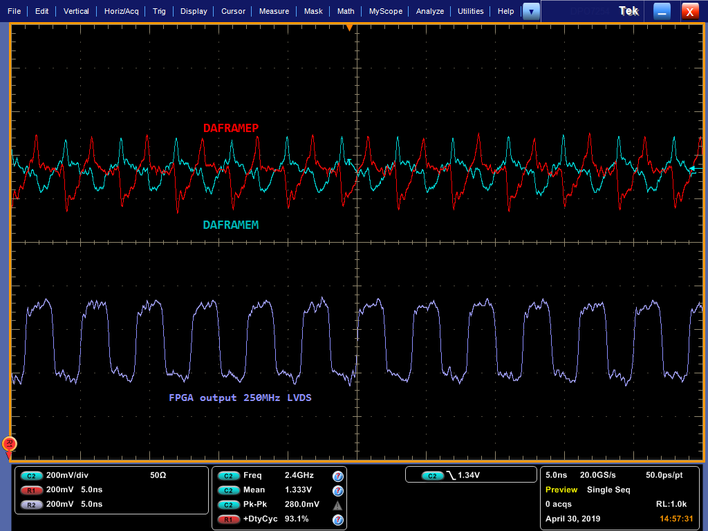
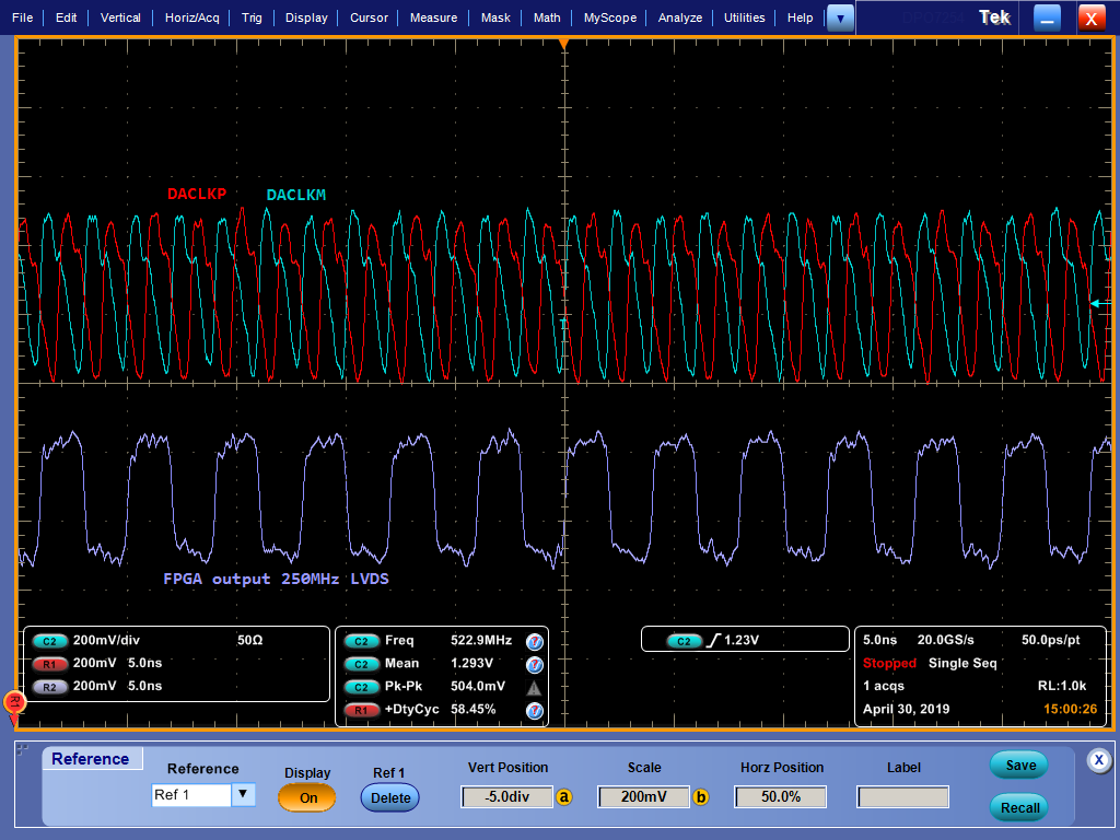
We measured the ADC output signals by single oscilloscope probe (TAP2500). Currently we can measure only one signal of the differential pair at a time as we only have one probe. Therefore phase alignment of positive and negative signals is not accurate as they are measured separately.
Take a look at the attached images. There are two measurements – ADC frame output measured directly at ADC pins, and DACLK measured approx. 3 cm (1.1 inch) away from ADC. On both pictures there is also measured LVDS signal generated by FPGA (violet trace), to check if the probing is adequate - we would expect something like that.
The initialization sequence on our design:
1) Generate positive hardware reset impulse with length of 250 ns.
2) Write ADC registers as (address, value)
WriteRegADC(0x08, 0x01); // ADC software reset - self clearing bit
WriteRegADC(0x06, 0x81); // clock divider by 2
WriteRegADC(0x08, 0x08); // disable control pins
What we have tried and looked for so far:
1) We have checked the schematics of our design with respect to the evaluation board – very similar, no significant differences.
2) We have checked supply voltages with the high speed probe – no problems observed, clean, no spikes, within specified tolerances.
3) We have tried to set the double strength of the LVDS buffers by setting the LVDS DATA STRENGTH register bit. This resulted into higher voltage swing but not changed the signal shape.
4) We have tried to change clock division to factor of 4, but we have not observed improvement in the signal shape (frequency did go half).
5) We have changed the interface to DDR LVDS to lower the interface frequency, but without improvement.
6) We have read out registers (from address 0 to 0x20) to verify settings of the ADC – all registers set as expected. There is non-zero value in few undocumented registers.
7) We cut PCB traces of one pair and soldered on 0402 100ohm termination resistor and measured at that resistor. Signal changed a little bit towards better shape, but its still pretty bad.
Questions:
1) We noticed the output common mode voltage is 1.25V. The datasheet specifies OCM voltage as 1.05V. Could this signify any specific problem?
2) Is there any power sequence that should be followed? We haven’t found anything in the datasheet, so we do not perform any power sequencing.
3) Is there any special procedure to correctly initialize the ADC if there is input clock of 500 MHz and we need internal clock division by 2 ? Please note that our 500 MHz clock comes from oscillator and transformer and is applied on the ADC clock input simultaneously with the ADC power-up. That means the ADC is clocked at 500 MHz clock at the beginning until SPI configuration is done, (default divider value is by 1).
4) Page 39 of the datasheet states that LVDS output swing can be set by the LVDS SWING register, but we cannot find any LVDS swing register in the register map. Could you please tell us what is the address the LVDS SWING register and what is the procedure to change the swing?
We would appreciate any comments, explanations, suggestions what could be wrong.
Thank you very much for your help.
Best regards,
Jan