This thread has been locked.

If you have a related question, please click the "Ask a related question" button in the top right corner. The newly created question will be automatically linked to this question.

ADC12D500RF: Question for Resolution and VIN+/- Power

Part Number: ADC12D500RF

As shown in the figures below, when input is 3dBm, the acquired data range is about +/- 1500.

When the input is 6dBm, the acquired data range is about +/- 2048(Meet the resolution shown in the datasheet, 12bits).

When the input is 7dBm, the data acquired range is about +/-2048 as well. However, the waveform has been cut at peaks and valleys.

Question 1: Why can the resolution reach 12 bits(acquired data range:+/-2048) when the input above 6 dBm? In my understanding, it's supposed to be 12 bits at any input power.

Question 2: Why did the waveform being cut at peaks and valleys when the input above 7dBm? The VIN+/- power is at least 15.3dBm. In my understanding, it's supposed to be cut when VIN+/- power over 15.3dBm.

Sincerely,

LB Shi

  • Hi LB

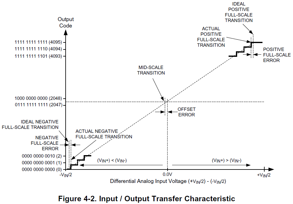
    The ADC12D500RF device will digitize the differential input that is presented according to Figure 4-2. Input/Output Transfer Characteristic. (Offset binary format shown).

    If the input voltage is approximately 0.0V differential, the output code will be around 2047 or 2048 decimal.

    If the input is a positive differential voltage less than the positive full scale level the output code will be between 2048 and 4095 and the Over-Range output will be 0. (ORI for the I-converter and ORQ for the Q-converter)

    If the input voltage is positive and at or above the positive full scale setting the output code will be 4096 and the Over-Range output will be 1. This is why the positive portion of the waveform is flat (clipped) while the input signal is above the positive full scale range of the ADC.

    Similarly, if the input is a negative differential voltage smaller than the negative full scale level the output code will be between 2047 and 0 and the Over-Range output will be 0.

    If the input voltage is negative and at or below the negative full scale setting the output code will be 0 and the Over-Range output will be 1. This is why the negative portion of the waveform is flat (clipped) while the input signal is below the negative full scale range of the ADC.

    Please note that applying signals beyond that specified in the Operating Ratings table can result in reduced lifetime of the ADC. Applying signals beyond that specified in the Absolute Maximum Ratings table can result in immediate damage to the ADC.

    Best regards,

    Jim B

  • Hi Jim,

    Thanks for your great support.

    Another question, VIN+/- power full scale level is 15.3 dBm as shown in the figure below. Why did the ouput waveform is flat(clipped) when VIN+/- power is set at 7dbm?

    Sincerely,

    LB Shi

  • Hi Lianbing

    15.3 dBm is the maximum power that can be applied in normal operation without reducing the device lifetime.

    The full scale voltage is determined by the Full Scale Range setting (via pin control or register based Extended Control Mode setting). This is shown in the Converter Electrical Characteristics table in section 3.6 as the VIN_FSR parameter.

    In Extended control mode with the default setting of 4000h, the typical FSR is 800mVpp differential. With a 100 ohm input termination this is approximately -1dBm to achieve the full scale (just below clipping) with a sine input.

    This gives around 16dB of headroom (allowance for temporary over-range signals) between the normal full scale input signal level, and the maximum operating RF power level.

    I hope this is helpful.

    Best regards,

    Jim B