This thread has been locked.

If you have a related question, please click the "Ask a related question" button in the top right corner. The newly created question will be automatically linked to this question.

ADS1234: Constant value read irrespective of the ADC input

Part Number: ADS1234


Hi

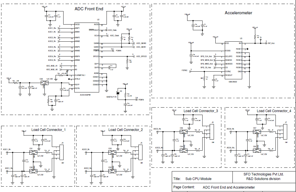
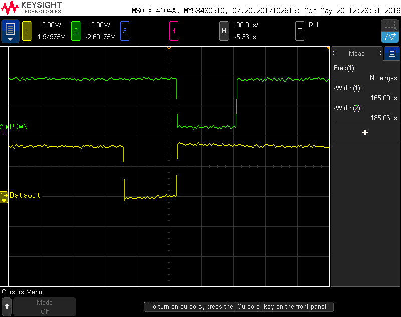
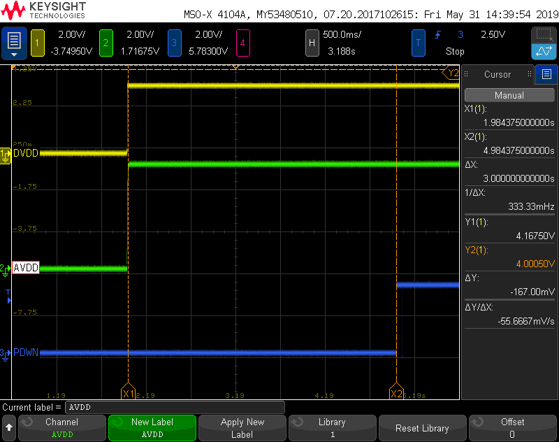
we are using ADS 1234 in our design for a load cell weight measurement system. The ADC works is working fine but in some power up the device is reading constant value 7FFF irrespective of the input variation.This issue is causing lot of trouble in our system.Please help us on this.The powerdown pin recommendation is followed in the firmware.Please share any other fix that could solve the issue

Thanks

Abin

  • Hi Abin,

    We have found that in some situations the device may not initialize properly on power up.  We are in the process of updating the ADS1234 datasheet with this additional information.  The suggestion is to pulse the PDWN pin after the device is in the operational state.  The best way to know that the device is operating is to wait for the first DRDY/DOUT transition from high to low, then pulse the PDWN pin from high to low and back to high.  The PDWN low time must be at least 26us (t14 time from Figure 41 of the ADS1234 datasheet).  This procedure will issue a complete reset of the ADS1234.

    Best regards,

    Bob B

  • Dear BOB

    Thanks for your response.we tried the same and still the issue is not resolved.Please help on this

    Regards

    Abin

  • Dear Bob

    The adc value read is having a fixed offset in some power up and variation is always from that fixed offset.The offset vary's in some power up and it is not evident in all power up's.This makes the calibration difficult for us.Please help on this

    Regard's
    Abin
  • Hi Abin,

    After pulsing the PDWN pin, are you issuing the Offset Calibration? If the ADS1234 powers up in an odd state, the PDWN pin will reset all of the device except the offset calibration register contents. The reason for not resetting the offset value is if the PDWN pin is used as a power-down pin only, it would not be useful to have to issue the offset calibration each time you bring the device out of the power-down state.

    However, if the intention is to reset the device, then you should issue the offset calibration (by sending at least 26 SCLKs) after the reset of the device and after the first DRDY/DOUT occurs following reset. The offset calibration process is shown on page 20 of the datasheet.

    So, power-up the device and wait until the device is fully operating (best known when DRDY/DOUT transitions from high to low state), pulse the PDWN pin, wait for DRDY/DOUT to transition from high to low state, then issue 26 SCLKs to start the offset calibration. The next DRDY/DOUT transition from high to low state should have valid conversion results.

    Best regards,
    Bob B
  • Hi Bob

    we have tried everything exactly as above except the gain setting.In initial power up the PDWN pin is held low by the MCu and gain is set to 128 and sampling speed is set high.Then everything is as mentioned as in your reply.Still we are fixed offsets.Any other timing need to followed for PDWN pins or SCK .Please help on this
  • Hi Abin,

    Please send me your schematic and pictures of your setup. It would also be helpful to see scope or logic analyzer shots of the communication. Also send me the output codes you are seeing and what you are expecting.

    Make sure that the offset is not real based on a missing reference voltage or input outside of the common-mode input range.

    Best regards,
    Bob B
  • Hi Bob

    Please review the schematics of ADC section.Diode and cap on PWDN pin is not installed.The fixed offset issue is resolved after giving a 3 sec delay in the code initialization as we suspected the issue is with power stability.But now there is a small drift in the reading and keep on increasing with time.Is there any such issue seen earlier with this ADC.

    REgards
    Abin
  • Hi

    The offset issue is not resolved completely.It is seen in some devices and reset wont clear the problem.

    Regards
    Abin
  • Hi Abin,

    If you have some sort of power-up issue with the ADS1234, then you must pulse the PDWN pin to reset the device. However, the PDWN pin does not reset the offset calibration register value. There is a good reason for doing this as the PDWN pin also functions as a power-down pin and you would want to keep the same calibration settings once you power-up the device by setting PDWN back high. So when desiring to reset the ADS1234 you should also issue the offset calibration to reset the value in the offset calibration register following the pulsing of the PDWN pin. If there is bad data in the offset calibration register (garbage), you want to make sure that this has been cleared and set to the proper value otherwise you will see an undesired offset in your result. The offset calibration is initiated by sending 26 or more SCLKs. The easiest way to do this with a micro is to read 3 bytes of conversion data (24 SCLKs) and then transmit an extra byte of SCLKs. This will initiate the offset calibration. The next falling edge of DRDY/DOUT should have valid conversion data.

    As far as seeing drift, this can happen as the supplies settle (which also includes the reference) and temperature drift from the ADS1234 self-heating. The most obvious drift related to self-heating will relate to the offset drift. Again issuing 26 SCLKs or more will re-calibrate the offset of the ADC. This can be done at anytime, and as often as necessary to cancel the offset drift effect.

    Another drift effect is possible from the analog inputs as it relates to analog settling. I can't read from the schematic what the input filter resistor values are but you have 1uF EMI filter caps followed by a differential cap of 100nF. I think the bigger concern is the reference input filter. It appears that the input filter resistors are 100k followed by the 1uF EMI caps and a 2.2uF differential cap. 100k input resistors are way to large of a value and the reference settling can take 10 seconds to fully settle. The concept is to make a ratiometric measurement whereby the excitation voltage is the same as the reference voltage. Any drift in the excitation will cancel out of the measurement. However if the filtering is much different between the analog input and the reference, any change or drift of the excitation source will appear differently in time. If the reference is more heavily filtered than the analog inputs it will take time for the reference to settle with respect to any change or variation in voltage. So try to match the analog input filters and the reference filter to be similar.

    Another drift component is the load cell itself as it will also self-heat and the excitation wiring in a 4-wire load cell be a contribution to the measurement.

    Best regards,
    Bob B
  • Dear Bob

    Will try the modification in hardware and try for the issues related to the drift.But the major issue is the higher offset.we provided 3 sec delay, pulsed the PWDN after the ready pulse and done self calibration in all the power up.Still we observe the issue randomly.The weight measurement will show 1000 Kg or some higher value without any weight on the load cell.Will ADC IC damage by trying out so many reset sequences.

    Also is it required to do offset calibration periodically?

    Regards

    Abin

  • Hi Abin,

    Please realize it is very difficult for me to troubleshoot your system without ever seeing it or knowing the details.  You are very familiar with what has been done and tested, but I am not.  So please share with me as many details as possible.

    I have done exhaustive testing of the POR circuit powering up and down the circuit literally hundreds of thousands of times during those tests. I doubt that you could have damaged the device from your testing unless you have exceeded the absolute maximum ratings for the ADS1234.

    I do not know what 1kg means in relationship to the system, so it would be helpful to know the load cell parameters like capacity and sensitivity (mV/V).  I would also like to see the raw code being returned to make sure that you are calculating correctly.  For example, many customers get confused with binary 2's complement and applying the conversion result (that is 24-bit) to a 32-bit value within the code.  In essence the code 0xFFFFFF in binary 2's complement is -1 in decimal.  Your result should be stored to a 32-bit signed (and not unsigned) integer and would initially be stored to the variable for this given example as: 0x00FFFFFF.  In decimal this would be represented by the value 16,777,215 which is not -1 as it should be.  There are many methods that can be used to extend the sign.  Basically if the most significant bit of the conversion result is 1 (1000 0000 0000 0000 0000 0000 in binary) then the value is negative and you must make sure that the MSB of the integer properly shows the proper sign.  If we have a signed 32-bit variable called code and it is determined that the value of code should be negative, then:

    code = code | 0xFF000000;

    where the sign bit is extended properly.

    Instead of just guessing, it would be helpful to have more details about the tests and raw code values after doing the PDWN pulse and offset calibration.  Other information that would be good to know:

    • Do you have scope or logic analyzer shots of the startup process (showing PDWN, SCLK and DRDY/DOUT)?
    • Is the offset seen on all four of the load cells or just some of them?
    • Have you measured externally AINP to AGND, and AINN to AGND to make sure there is no common-mode violation?
    • Have you measured VREF at the ADS1234 input pins to verify this is as you would expect?
    • Can you share with me specifics on how you are testing (and perhaps some pictures of the setup)?
    • Have you verified that there are no issues with wiring or contact issues with connectors?
    • Have the tests always used load cells, or have you tried creating a resistor bridge or shorted the inputs using a voltage divider to narrow the scope of the issue?

    As you can see there are many things that I don't know that could help in identifying the issue.

    Best regards,

    Bob B

  • Dear Bob,

    1. As per your request , Waveform of PWDN pulse, Offset calibration and data reading has been attached for your reference to detail the start up process.

    2. Yes , the offset are seen on all the four channels and offset values are almost same on each channel. in Our design both excitation voltage of load cell and ADC reference voltage are 5V. The load cell is having a sensitivity of 1 mV/V ( here the capacity is 50 kg, so max. output from load cell for a fully loaded condition would be 5mV and we are running the ADC with a gain of 128, thus max analog input range of ADC would be +-17 mV something. The typical values of offset we got are 194 kg. 120 kg, 38 kg on each load cell and these values are not provided by the load cell that we confirmed by measuring the voltages across load cell output wires..) Datasheet of load cell is attached.

    3. yes we have measured voltages on AINP and AINN with respect to GND and its value is 2.5V and is not violation to common mode voltage range of ADS1234.

    4.yes we have measured and expected voltage of 5V obtained.

    5. We can't share actual test setup as it highly confidential. But I can assure test setup is not affecting data capture as we are getting correct reading when a weight is placed on the load cell.

    6. there is No wiring or connector damages.

    Regarding the data calculation you have mentioned above, our Firmware team have confirmed that the calculation method is same as that of your suggestion and we could correctly convert the output from ADC chip to weight for both positive and negative inputs.

    DataReady Vs PDWN pulse

    Offset calibration with 26 clock pulses

    Data reading, Error data is obtained

    Load cell datasheet( 50kg)

  • Hi Rino,

    Welcome to the E2E forum! The second scope shot is not clear. There may be some number of issues with probe grounding or connections, but PWDN is showing low, and the SCLK is very noisy. The minimum low/high time for the SCLK is 100ns. This appears to be in violation even though the SCLK frequency is quite slow. Can you explain the differences as to why some of the plots are very clear, while the one I'm referring to is poor? Are all the plots being probed at the same place? Has the timing been verified to make sure the offset calibration has actually taken place?

    Best regards,
    Bob B
  • Dear Bob,

    please refer the attached scope shot of offset calibration clocks. I think all the timing constraints of clock pulses are met.

  • Hi Rino,

    This scope shots is much improved over the one shown previously.  As we have not clearly identified what is actually happening at the ADC, I want to make sure I fully understand the current situation. 

    Initially the issue was seeing 0x7FFFFF (positive full-scale) occasionally on power-up.  This original issue was apparently resolved by pulsing the PDWN pin.  A new issue now occurs where occasionally on power-up there is an offset.  Is my understanding correct so far?

    At one point with some devices, if the startup was delayed by 3 seconds the offset issue was removed.  This may mean that the AVDD supply is coming up slower than the DVDD supply.  When AVDD and DVDD are not the same supply, then the PDWN pin must stay low at least 10us after AVDD supply has reached nominal voltage.  See the note in Figure 40 of the ADS1234 datasheet.  

    After PDWN goes high it should take about 402ms before DRDY/DOUT transitions from high to low.  This will signal that the device is operational.  At this point toggle the PDWN pin to reset the ADS1234.  After PDWN goes back high, DRDY/DOUT will be high for about 402ms then goes low.  You can capture this data read on the scope while issuing the additional clocks for the offset calibration (26 SCLKs total).  This scope shot would be good for me to see.  The calibration will take about 803ms from the last falling edge of SCLK and is signaled complete when DRDY/DOUT transitions from high to low.  Again, capture this data on the scope and please send both of these shots to me so I can see if the calibration is truly taking place.  You should also see the timing as described above to also help verify.

    If the above steps are followed the ADS1234 should be giving valid results.  However, there are a few assumptions.  One is the AVDD and DVDD supplies are settled and operating at their nominal voltages.  Second assumption is the reference is fully settled.  Third assumption is the analog inputs are fully settled.

    I commented some number of posts back regarding the long settling delay on the reference input due to the very heavy RC filters.  If you are still seeing some issues, I would suggest to try again by replacing the input resistance on REFP and REFN with 0 Ohm resistors .  If these are 100k as shown, these are too large of a value for the reference to work properly.

    Best regards,

    Bob B

  • Dear Bob,

    Please see below attached Images showing the timing requirements suggested in your previous reply.

    Please note that we have been Configured the ADC in High speed mode , that is 80 SPS , so that the time delays would be different and is given in ADS1234 datasheet.

    One more point is, after providing an initial delay of 3 seconds for PDWN to go high after settling both DVDD and AVDD, the offset issue is resolved without any offset calibration pulses. We need clarification whether Offset calibration is required or not. because without giving the above 3 seconds delay, there has been high offset value even with offset calibration.

    DVDD Vs AVDD settling delay

    3 Second delay for PDWN after AVDD is settled

    DATARDY High to Low transition after PDWN goes to High(1st Transition)(63 ms delay)


    DATAREADY LOW PULSE (840 us)

    PDWN Low Pulse ( 180 us)

    DATAREADY High to Low transition after PDWN pulse( 54 ms delay)

    DATARDY High to Low transition after Offset calibration last pulse( measured delay is around 100 ms as given in datasheet)

    Best regards,

    Rino Michel

  • Hi Rino,

    Thanks, this is excellent information! You are correct with the timing. I was assuming 10sps, and if you are using 80sps then you would adjust the timing as shown in the ADS1234 datasheet. From the scope shots I see normal activity and the proper timing which shows the device is powering up properly. The offset calibration is important at startup to remove any device offset from the PGA and modulator stages. If you can accept the +/- 1ppm of FS offset error in your measurement, then you would not need to issue the offset calibration. However, I would still highly recommend it.

    As to waiting 3 seconds, this seems to be very unreasonable but may be required based on analog settling. I have yet to hear definitively how you are powering the reference inputs. Based on the schematic I reviewed earlier I saw there was 100k resistors and 2.2uF differential cap. The RC time constant (200k*2,2u) is 0.44s. 5 time constants would be about 2.2 seconds. As the reference would need about 17 time constants to settle to a good value you would need about 7.48 seconds total for the reference to settle. So from this calculation I can see that it would take about 3 seconds for the reference to settle to about 98%. If there is 100k series resistance for your filter inputs, then I would strongly suggest lowering these values. Also, there will be a small bias current drawn from the reference which will place a voltage drop across the input resistor creating an error. I would suggest that the reference filter resistor value be in the range of 1 to 5k.

    With the proper startup sequence, the ADS1234 should operate as expected. PDWN should only go high after DVDD has reached nominal operating voltage (16ms). Issuing the offset calibration is not required, but highly recommended. Limiting the settling time of the reference is also highly recommended.

    Best regards,
    Bob B
  • Dear Bob,

    Thank you very much for your quick reply.

    Regarding reference input voltage settling time your calculations were correct. But the thing is that, our entire system takes about 10s to complete boot up then only it displays wieght values, so that the reference input time will not affect the correctness of the reading, even if it affects how can this affect in such a way that the ADS1234 is giving a very high value on all the channel's as given in the previous replies( like consistinctly giving weghts lik3 153kr 34kg on each channel and giving a proper output variation when a weight does).

    As per your suggestion we have changed the series resistor from 100k to 100ohm but this change is done only after providing 3s delay.

    anyway by providing those 3 s delay , our system working fine now without any offset calibration. You can share any points that i missed to ifentify the rooy cause of ADS1234s behaviour.

    Regrads

    Rino Michel