Other Parts Discussed in Thread: ADS54J66, ADS54J66EVM,
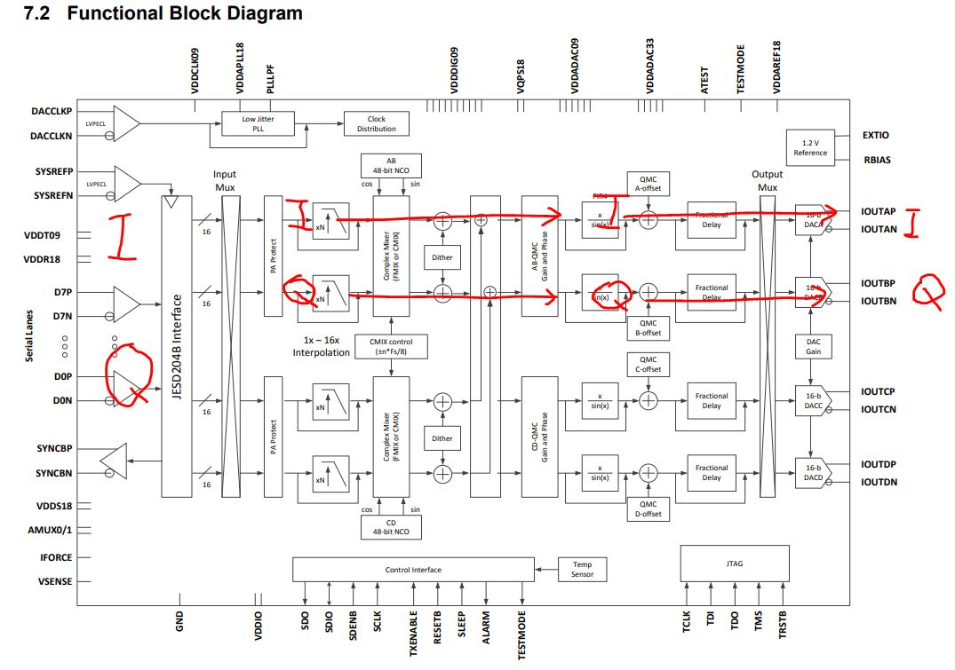
1)the datasheet provide page 31 table 10 says JESD204B Frame Assembly Byte Representation(LMF:421) for dual channel,internal architecture page -24 functional block diagram says, A,B,C,D channels ,but in page 31 it say I0,Q0,I1,Q1,I2,Q2,I3,Q3, that means each individually chaneel is consider as I and Q and what will be maximum out of the dac if the sampling of the dac is 2.5Gsps
2)in functional block diagram page -24 we have seen the in put muxing and out put muxing in the devices is this are configurable,ie means can we same Data to all the dac out put are these data can be interlived also.