This thread has been locked.

If you have a related question, please click the "Ask a related question" button in the top right corner. The newly created question will be automatically linked to this question.

ADS114S08: Cannot use the same pin for the + PGA input and the excitation current source

Part Number: ADS114S08
Other Parts Discussed in Thread: ADS1148

Hello,

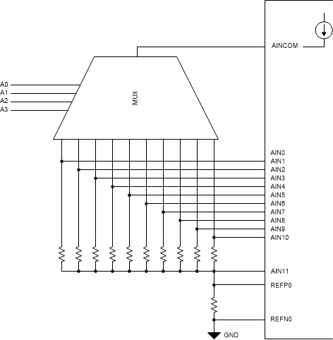
In a recent design, we migrated from the ADS1148 connected to 7 RTDs to the ADS114S08 so that we could measure 10 RTDs. To utilize so many channels on these chips you have to use the same pin for the + PGA input as the excitation current in a two-wire configuration for each RTD. Below is how we're wired for one of the RTDs:

This worked well with the ADS1148, and the temp measurements were reasonably accurate. When we try this with the ADS114S08 (no filter resistors), the temp measurements are high by 10-15 degC. After some playing around with a fixed resistor in place of the RTD and measuring voltages with a DMM and comparing that to the ADC digital output, it became clear that there must be resistance (switch resistance?) on the order of 50 ohms inside the chip between the output pin and the MUXs that connect the PGA+ and the iDAC to that pin. To prove this, I wired a different external pin to the pin that is connected to the PGA+ pin and routed the current source through that, so that the IDAC current exits the chip first and then flows across the RTD with dedicated pins across it for the PGA+ and PGA- connections. This fixes the problem, and must be because now that 50hm resistance in series with the current source doesn't matter because the PGA+ pin is connected on the other side of it - after it has exited the chip.

I guess my question is, can you confirm that there's that much series resistance (~50 ohms) to the output pins, and that the ADS114S08 should not be used in a two-wire configuration where the same pin is used for both the PGA+ input and the excitation current? None of the application notes have this part connected like this, and maybe that's a clue. In the design note sbaa329, the #2 design note on page 2 says not to have the ADC input pin be the same pin as the excitation current, but it blames the filter resistors as the reason not to do it. But we don't have filter resistors in our design.

This is disappointing because it means that the max number of RTDs you can connect and get a reasonable measurement on is 6 because you need an extra pin for the excitation current for each RTD you're measuring. And I'm not comfortable calibrating that large error out because that (switch?) resistance will change over temperature and add to the error. (When I put my finger on the ADS114S08, I can cause a small drift in the temperature measurement when we use the same pin for PGA+ and excitation current. When they are separate pins, no visible drift in temp reading happens when I put my finger on the chip.)

Please let me know if my conclusion is correct, or if you think I just may have a bad part. Thank you!

Phil

  • Hi Phil,

    Unfortunately your diagram did not come through in your post.  Most likely what you are seeing is internal trace resistance at the point of the IDAC mux to the pin on the ADS114S08.  This can actually vary some from analog pin to pin based on distance and routing.  The IC designer is estimating this to be around 30 Ohms on some of the furthest pins from the mux.  Figure 49 on page 30 of the ADS114S08 datasheet is a pretty good representation of where the switches are located in relation to the PGA input.  The IDAC output connects directly to the pin, but there will be some resistance from the IDAC mux switch to the pin.  The voltage drop across this trace will be measured by the ADC.

    I'm rather surprised you do not see this same effect on the ADS1148.  It is possible that there is better routing by using fewer inputs that will allow for shorter distances and thicker traces from the mux to the pins which would lower the  resistance.  There may also be a star type connection at the pin, but unfortunately I do not have access to the design files for comparison.  In simulation I've often seen 20 Ohms as the trace resistance.

    Although it is theoretically possible to drive current out the same pin as is being measured it is often impractical to do so.  In fact we discourage this type of usage due to noise concerns.  Without adequate input filtering external noise can alias back into the passband which can add noise into the measurement.  So in many, if not most, there would be input filters required.

    It should be possible to drive current out a single pin to drive all 10 RTDs.  The current would go through an external IDAC mux to route the current to the appropriate RTD.  I have a simple diagram below to illustrate what I'm talking about.  The diagram does not show any input filters, but rather a basic connection diagram.

    Best regards,

    Bob B

  • Thank you for the quick response... That makes sense. I didn't do the same test where I route the current source out to a different pin on the ADS1148. I'm sure I'd see some difference, but the temp measurements were within a couple degrees C (using a 3.0k metal foil resistor as the reference and a 1k platinum RTD) so I never worried about it. But using the same values (3.0k reference, 1k RTD) with the ADS114S08 is so far off (10 to 15 degrees C) that it made me investigate further. They must have done something to get that resistance way down with the ADS1148. And there are app notes that show using the same pin as PGA+ and iDAC current in a 2 wire system. (sbaa180b.pdf, two wire RTD example).

    Again, thank you for your response. Will TI please update the data sheet with a note that discourages using the same pin for PGA input and excitation current, since the ADS114S08 really wasn't designed for that?