This thread has been locked.

If you have a related question, please click the "Ask a related question" button in the top right corner. The newly created question will be automatically linked to this question.

ADS1298: Connection Schematics

Part Number: ADS1298

Hello,

I am implementing a circuit for sensing 8 biological signals (EMG) in differential mode using one ADS1298. My intention is to have a unipolar power supply of 1.8V for DVDD and 3.3V for AVDD (which will be supplied by an ODROID), to use an internal voltage reference and no electrode for RLD. The connection to the ODROID is through SPI with the 4 regular communication channels.

I am wondering if someone can check my schematic (attached) and help me in the case there are errors? I am especially concerned with the ADS pins 35, 52, 60, 62. I will not exclude errors in other pins...

If there is any extra information that I forgot to give, please ask.

Thank's in advance,
Best,
Sofia Rafael

P.S. In the schematics, the conditioning circuit at the left is repeated for each of the differential inputs

  • Hello Sofia,

    Thank you for your post and welcome to our forum!

    1. Pin 35 is ok. This will disable power-down. 
    2. Pin 52 is ok. This will select the internal master clock.
    3. Pins 60 and 62 can be shorted to AVDD if unused. Leaving them floating is not detrimental, but tying them to AVDD generally reduces noise coupling and leakage current.

    The input signals appear to be AC coupled at the amplifier outputs, but there is no DC biasing for the signal. The inputs to the ADS1298 must remain within the specified input common-mode range in the datasheet. Typically, a resistor divider or pull-up to RLDOUT is used to bias each input near mid-supply.

    Best regards,

  • Hello Ryan,

    Thank you very much for your quick response and the time you took to go through my question.

    First, in reply to your last comment, I thought that the resistors that I have connected in pin 63, and after the capacitors in series with the input channels did the trick of "Setting Common-Mode Without Using RLD Electrode". It is not very clear in the image but for each of the inputs I followed fig 95 in the datasheet. Is it correct or should I do it in another way?

    I have another question regarding pins 27 and 29 of the ADS. Can they be left in a floating state?

    Thank you very much in advance,
    Best,
    Sofia Rafael
  • Hi Sofia,

    Apologies if I misread the schematic. It's difficult to see where the left side of each 10-M resistor is going, but if you're following Figure 95, that will work fine!

    At the output of each amplifier, you have 100 nF of capacitance in series (i.e. C10). This series cap forms a high-pass filter with the 220k resistors to ground (i.e. C9). The cutoff appears to be a little high = ~7.23 Hz and could be reduced, but the signal bandwidth you require is really up to you. Furthermore, after the low-pass antialiasing filters (i.e. R7 and C7), you have another 1 uF of capacitance in series with the inputs (i.e. C6). I don't believe you need these 1-uF caps since the inputs are already AC coupled.

    I believe the correct approach would be to remove the 220k resistors to ground and connect each input to RLDOUT through 10M ohms after the 100-nF capacitors. Then you can keep the low-pass filters and connect to the ADC inputs directly.

    Regards,
  • Hello Ryan,

    Thank you very much for your feedback it was really helpful.

    Best,
    Sofia Rafael

  • Hello, 
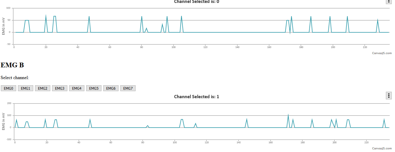
    Using the confifuration above I am getting some strange behaviour when I try to implement the internally generated test signal.
    The results I am getting so far are these: 
    The peaks are around 60mV. I was expecting to get a square wave with freq 0.47Hz and 1mV or 2 mV. 
    After the initial power up I read the correct ID of the ADS1298, then I am sending the OPCODES:
        spi.write([SDATAC])
        received = spi.transfer([WREG, CONFIG3, 0x00, 0xC9]) # C9 = 1100 1001
        received = spi.transfer([WREG, CONFIG1, 0x00, 0x64]) # 0110 0100
        received = spi.transfer([WREG, CONFIG2, 0x00, 0x30]) # 00110000
        received = spi.transfer([WREG, CHnSET, 0x00, 0x05])
        spi.write([START])
        spi.write([RDATAC])
    Then I set a function for detecting toggles in the DRDY.
    I have tried changing the speed of the SPI communication (200KHz, 1MHz, 3.9MHz) the results haven't changed. I have 
    SPI in mode_1; 
    CPHA = 1;
    CPOL = 0; 
    Reading of 8 bits per word
    My conversion to mV is like this:
    Vref = 2.4; Gain = 6; bits_per_channel = 24
    LSB = ((2*Vref)/Gain)/(2**bits_per_channel-1) # Volts
    Then I XOR the 3 bite reading with 0x800000
    milliVolt = ((code(decimal, result of the XOR)-1)*LSB/Gain)*1000
    Can someone please help me?
    Best wishes,
    Sofia
  • (sorry for the second message... )

    Here are some oscilloscope images for the SCLK, DRDY, DOUT, and CS that may be helpfull for the debugging.

    Yellow SCLK; Blue DRDY;


    Yellow SCLK; Blue CS

    Yellow SCLK and Blue DOUT

    I hope someone can help me. Thank you very much.

  • Hi TI experts,

    I still haven't solved this issue... Any suggestion is more than welcome.

  • Hi Sofia,

    In your first scope shot, it looks like your SPI communication is overlapping the occurrence of the next /DRDY falling edge. This would result data corruption as the old data is immediately overwritten with new data. You must send enough SCLKs to read all the data before the next /DRDY falling edge occurs in RDATAC mode. 

    It looks like your data rate is about 8.3 kHz and your SCLK is only 500 kHz. You could try either reducing the data rate or increasing the SCLK frequency. Also, there is a significant delay between the /DRDY falling edge and your first SCLK rising edge. Try reducing this delay to give yourself more time to read the data.

    Best regards,

  • Hello Ryan,

    I still haven't solved this issue. It seams a bit contradictory that I am having my data rate 8.3kHz when I set CONFIG 1 to have 1kSPS.

    So, is it possible that those configurations are being set to the default ones due to the CS signal going high after each data reading in the RDATAC mode like what is shown in the third image?

    I have tried setting CS manually to low after the reset pulse, but then DRDY doesn't signal that data is ready... Shouldn't it work?

    About the data ready, it is ready after the falling edge or does it have to wait for the pulse in DRDY?

    Sorry for keep bothering you and thank you very much for your previous input

  • I am also getting this MOSI signal in blue for the SDATAC signal, which from what is shown in the link bellow is not correct as it should stay high until the next OPCODE. Can this be the source of the problems? If so do you have any sugestion (I have a 220k in the line for the signal comming into the chip)? 

    e2e.ti.com/.../911701

    Again Ryan, thank you very much for all your patience.

  • Hi Sofia,

    If the data rate does not appear correct, I would advise fixing that issue first. There are some general debug steps listed in the BIOFAQ page that walk you through validating device functionality and communication. Remember that you cannot change registers without first sending the SDATAC command to exit RDATAC mode. Can you confirm whether you are using the internal master clock (2.048 MHz) or an external master clock? If external, what is the frequency?

    Toggling /CS between each SPI transaction will not affect the register settings. The registers should only return to their default state after a /RESET pulse or power cycle.

    Holding /CS low is also OK. This should not have any effect on the /DRDY pin. Are you controlling conversions using the START pin or are you using the START/STOP SPI commands (with START pin held low)?

    The data is ready to be read immediately when you see the /DRDY falling edge. It will be overwritten by new data just moments before the next falling edge.

    Best regards,

  • The SDATAC command looks correct to me. The "tail" at the is probably from the voltage discharging slowly due to the capacitor probe as the MOSI pin on your microcontroller goes low or high-impedance. As long a sit remains high enough during the SCLK falling edge, the ADC should read this bit correctly. The image in the post you linked is using a logic analyzer, so the waveforms are translated as digital high/low levels only.

    Regards,