This thread has been locked.

If you have a related question, please click the "Ask a related question" button in the top right corner. The newly created question will be automatically linked to this question.

ADS127L01: Spikes in Acquired Signal

Part Number: ADS127L01
Other Parts Discussed in Thread: THS4551,

Hi,

Thanks again for your help with our previous questions regarding ADS127L01. 

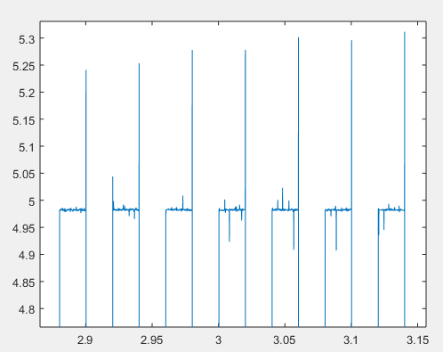
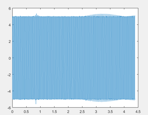
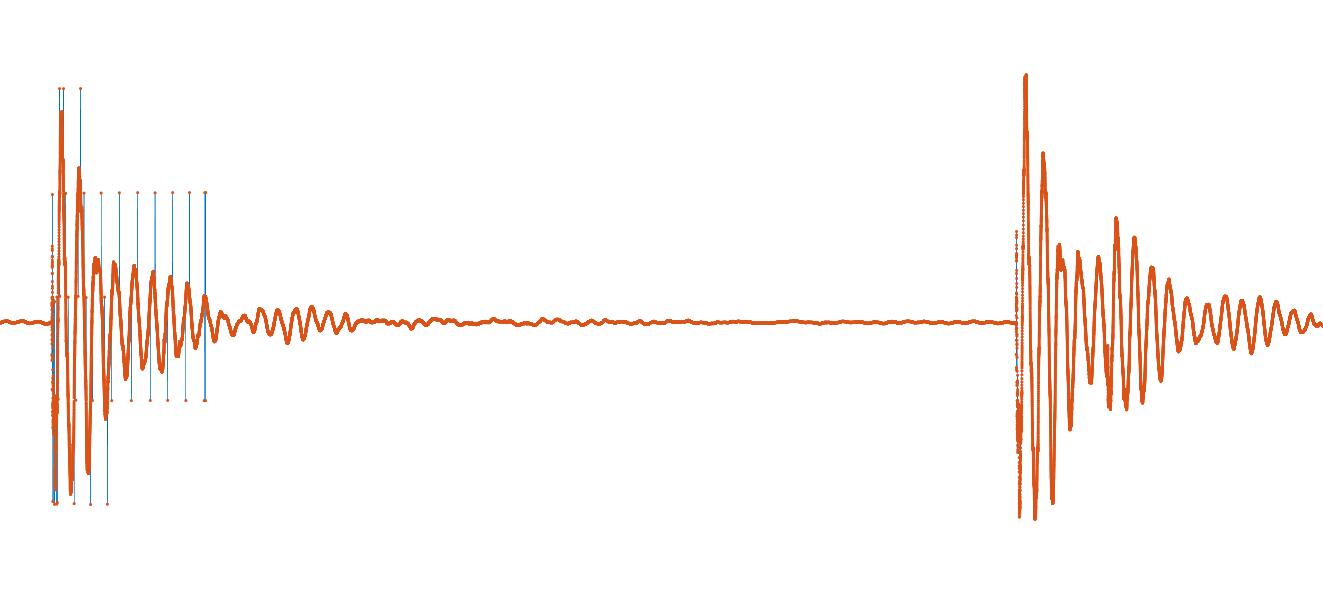
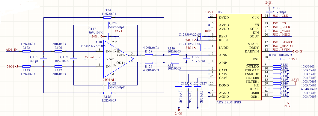
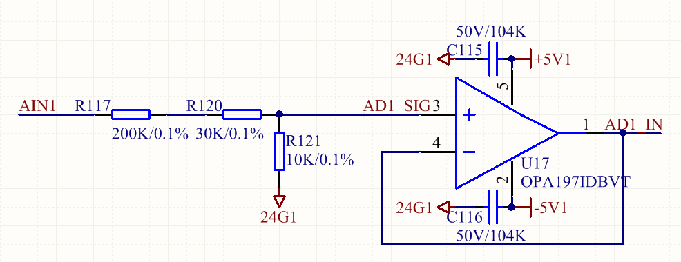
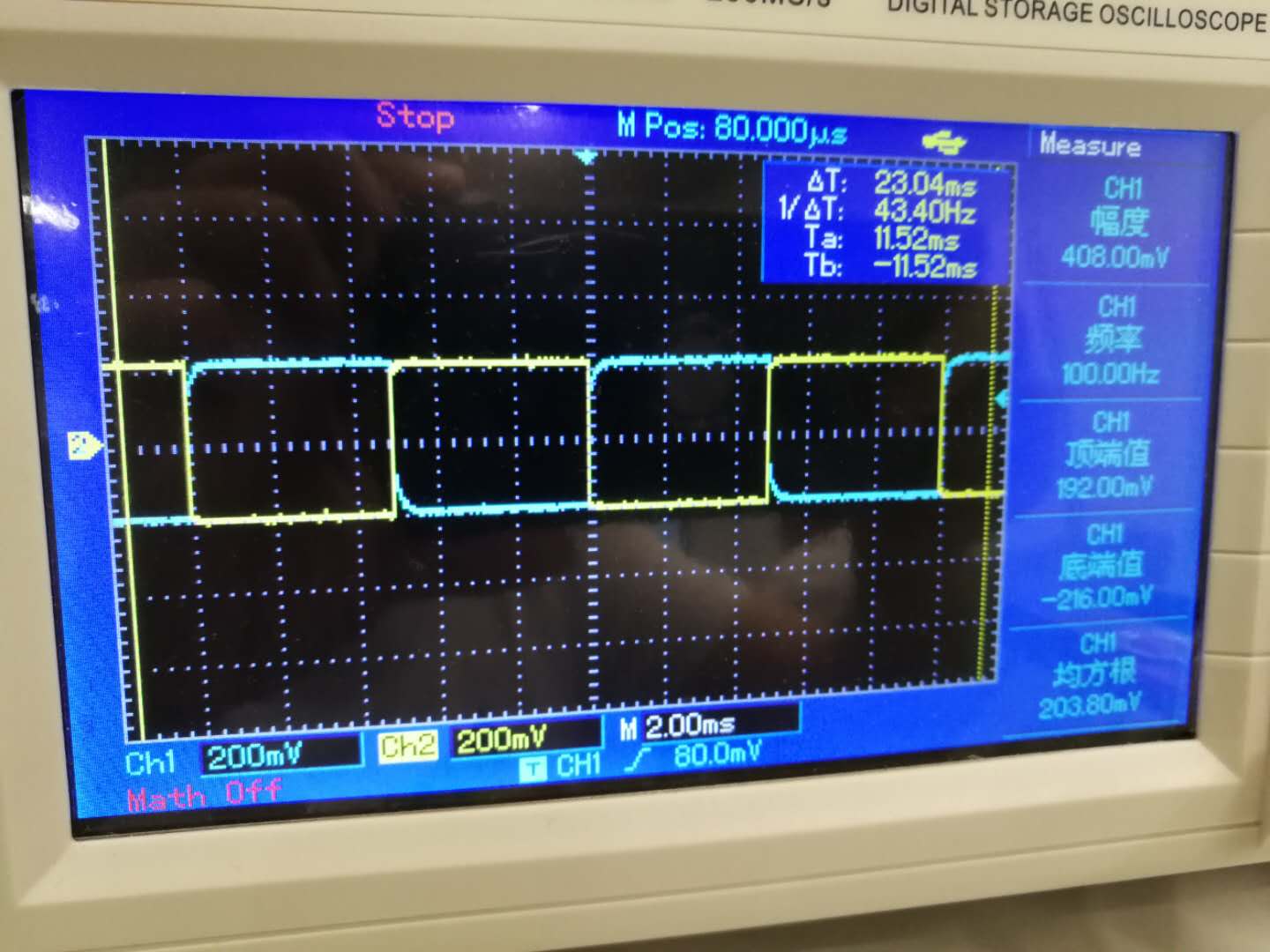
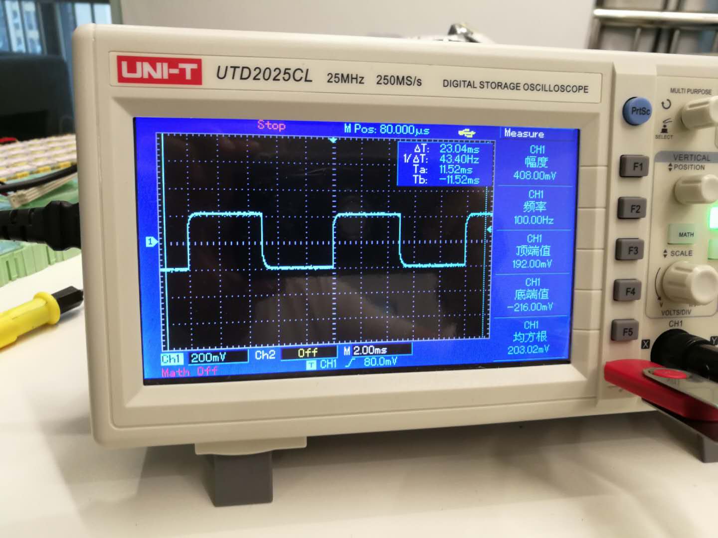
We now able to get digital data from the ADC. The ADC is operating at High Power Mode, using wideband 2 filter(0.45-0.55 Fdata). The AD is sampling constantly at 128kHz. We are using the recommended design with THS4551.

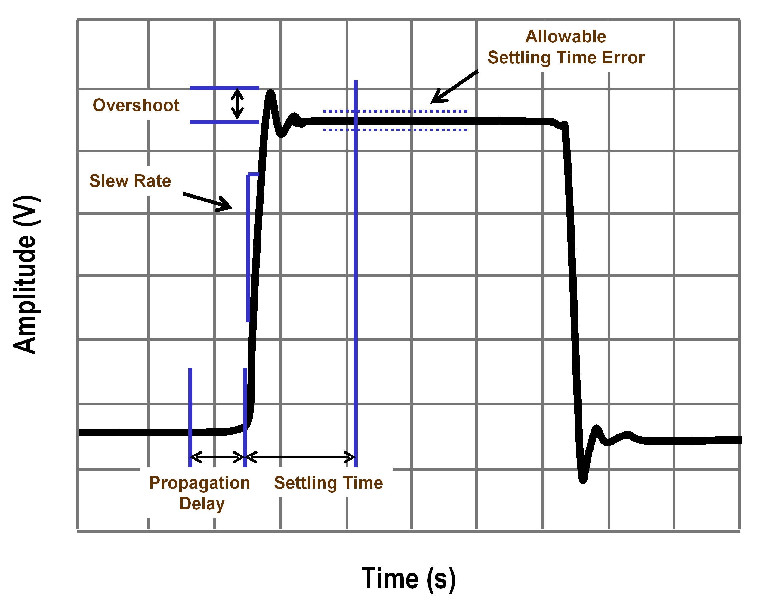
However, we observed unusual spikes in nearly all the tests. it is usually fine with sine wave input when the signal does not change abruptly, but with square wave and pules input, the spikes happens a lot. it seems that the AD need time to settle done. The AD connects to a xilinx Spartan 6 FPGA. We have ruled out the FPGA issue as well as the analog circuit issue before the ADC. 

Any clue on what the problem might be? how do we solve the problem. 

Thank you 

Ben

  • Hi Ben,

    Please provide a schematic showing the input amplifiers and ADC, as well as the reference voltage used. Also, what are the time scales for the above waveforms?

    When applying a step input (either square wave or pulse), the digital filter will have a long settling time when using the wideband filters. For example, when sampling at 128ksps, the filter will need about 45 samples or 352uS to settle to within 5% of the final value, and a total of 84 samples or 656uS to fully settle.

    Regards,
    Keith N.
    Precision ADC Applications
  • Hi Keith, 

    Many thanks for the quick response.

    The reference voltage is 2.5 Volts. the frequency for the square wave is 10Hz, we are sampling at 128kHz constantly. For the hammer input impulse signal, each impulse is about 0.3 second long. 

    I understand it may take 45 samples for the AD to settle to 5% of the final input value, we should see an oscillation/damping in the 45 samples. However, in many cases, we only see one point that is abnormal. So, I feel the settling period may not explain well the spikes, especially in the hammer input signal. We tried 5 times, and 3 out of 5 have the spikes in the signal.  and the curve seems to track the input signal very well. Please note we used the NI cDAQ to generate the hammer input so we know the exact input signal. In the hammer input signal, the spikes are single points rather than an settling curve, and they seem to be at a constant level, any clue?

    Attached please find the schematic.

  • Hi Ben,

    Thanks for including the schematics. It is not clear to me if this is a conversion issue or a signal conditioning problem.

    Can you measure the output of the THS4551 when using the square wave? Measure OUT- and OUT+ with respect to ground, 24G1. Ideally, the voltage should be centered around 1.65V (Vcom1 equal to 1/2 of the AVDD supply on the ADS127L01), and for a full scale swing, each output would range from 0.4V to 2.9V.

    Also, please confirm that you have good supply bypassing on the AVDD and DVDD pins of the ADC; at least 0.1uF in parallel with 10uF as close as possible to the device.

    Regards,
    Keith
  • Hi,

    We did the test as you suggested. With a square wave input, we measured the output at OUT- and OUT+ with respect to ground, 24G1.  We did not see any spike in the OUT- and OUT+ in the oscilloscope (See attached picture). I think this is reasonable. Any analog circuit has 'inertia', any abrupt change in the signal requires energy input, and the change is usually smooth rather than the abrupt digital value change we observed in the above pictures. 

    please Note, we used the Vcom1 = 1/2of REF1(1.65V) on the ADS127L01, the VCOM1= 1.25V rather than 1.65V. would this affect the result?

    We also confirmed we have good supply bypassing on the AVDD/DVDD pins, the 0.1uF and 10uF are very close to the device. We don't have floating pins or empty pins, all the pins are properly grounded. 

    We then did some research on google. the spikes in ADC output seems to be a common issue, perhaps due to the conversion issue or due to the timing of FPGA reading the data. what do you think? any suggestion? 

  • Hi Ben,

    The waveforms look well behaved. I assume these scope measurements were AC coupled? You do not need to send pictures, but please measure with DC coupling settings. You should see the waveform offset around Vocm=1.25V. (1.45V to 1.05V in the above waveforms)

    You can use the lower Vocm of 1.25V; you just need to make sure that neither output on the THS4551 gets lower than 0.1V with respect to ground (24G1). This will occur at your largest input voltage swing.

    I checked the filter response on the ADS127L01EVM. The Wideband filters show around 10% over/under shoot. I think this is the main cause of the overshoot that you see. For impulse or square wave inputs, I suggest you use the low-latency filter option. (pin 12 high, pin 13 low) This filter does not exhibit the over/under shoot.

    Regards,
    Keith
  • Hi Keith,

    We did try the DC coupling, and the signal was normal without any spikes.

    We will try the low-latency filter option, but I don't this is the reason. A typical overshoot has ripples (or damping). Overshoot/undershoot happens because we are using the sum of a limit number of sine waves to represents a signal, such as a square wave.  Ideally, we should use an infinite number of sine waves, and they would be no overshoot or undershoot. Mathematically, this is the Fourier transform of a time waveform into the frequency domain. Unfortunately, with digital signal processing, it is not possible to use an infinite number of sine waves, so they are ripples. and the amplitude of the ripples should be related to the amplitude of the original time waveform. 

    However, this is different from what we observed, especially in the impulse response, the spike values are almost constant, and they happens only at one point, with no sign of ripple or damping. this type of abrupt change is more likely from the digital side, maybe a shift position of the acquired data, either in ADC or in the FPGA, or a sampling issue, the FPGA is taking the data when the ADC is not actually ready yet.  What do you think?

    We will try the low latency filter, but I don't think that gonna help, I will keep you updated. 

  • Hi Ben,

    The host needs to monitor the /DRDY line when using SPI mode, and when it transitions from high to low, new data are ready to be read out of the device.  For the default configuration, you will need to clock out 32b of data and then idle SCLK low for at least 4 master clock periods before the next falling edge of /DRDY per Figure 91 in the datasheet.

    If you do not meet these requirements as well as the timing requirements in Figure 1 of the datasheet, then you could be getting corrupted readings.

    If you can capture the waveforms for /DRDY, /CS, SCLK, I will check to see if there are any timing violations.

    Regards,
    Keith