This thread has been locked.

If you have a related question, please click the "Ask a related question" button in the top right corner. The newly created question will be automatically linked to this question.

ADS1293: Few Clarifications Needed

Part Number: ADS1293
Other Parts Discussed in Thread: ADS1292, ADS1298

Hi,

1. In the ADS1293 EVM  the crystal circuit is shown as under

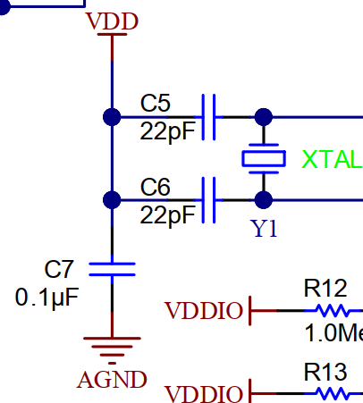
The crystal seems to be connected to AVDD and AGND, its generally the case that high frequency signals are connected to DVDD and DGND while the analog part is kept as quite as possible. So is this an error in the schematic?

2. The crystal oscillator circuit is different in the EVM and in the datasheet.

Which is the correct one. I'm attaching the snapshot from the datasheet since the EVM schematic is already shown above. (Although I must say even in the datasheet AVDD seems to be connected to the crystal)

3. The shield is generally driven with another op-amp via the RLD circuit. However the ADS1293 datasheet says that the CMOUT can be used as a shield drive. Do we still need an op-amp at the output of the CMOUT pin or can the CMOUT directly drive the shield?

  • Hi Alwyn,

    Thanks for your post.

    I tend to agree with you on the XTAL supply. Both XTAL1 and XTAL2 pins are listed as digital inputs, who's voltage should be limited to VDDIO, not VDD. The Absolute Maximum Ratings allow any input pin to range up to VDD + 300 mV, so we should not expect any damage to the device under those conditions on the EVM. Also, given that the supply voltage is AC-coupled to the XTALn pins, the amplitude seen at the pins may be even less. Thanks for pointing this out!

    You should not need an extra buffer for CMOUT to drive the shield. However, you should be driving the shield and the body to the same common-mode voltage. I believe it makes more sense to use RLDOUT for both in this case. There will be some phase delay between CMOUT and RLDOUT, but this does not have a significant impact on the CMR of the system.

    Best regards,

  • Hi Ryan,

    Thanks for your time and excellent answers!

    So to recap

    1. The supply given to the crystal should be DVDD and DGND, correct? I am trying to re-confirm becuase both the EVM and the datasheet show AVDD and AGND given to the crystal. Also is the extra cap shown in the EVM needed?

    2. Which of the 2 crystal schematics shown above is the correct one, or will both work just the same.

    3. For the shield drive you say that an external buffer is not needed, however I have seen several schematics like ADS1298 EVM and ADS1292 EVM which have buffers shown and gets an input from RLDOUT and then it drives the shield.

    So for the shield would you think that driving both shield and RLD from the RLDOUT pin will work out, will the RLDOUT pin have sufficient drive to get this done? So I have 3 options now
    a. Drive both shield and RLD from CMOUT.
    b. Drive both shied and RLD from RLDOUT
    c. Drive RLD from RLDOUT and shield from CMOUT. (But as you say this configuration might have phase mismatches)

  • Hello Alwyn,

    1. Yes, I think DVDD and DGND make the most sense as the supply voltages for the XTAL. The extra cap is not really necessary. If you think about it, this cap is just another decoupling capacitor on the VDD supply, of which there are several others in parallel.

    2. Same answer as 1.

    3. Option b makes the most sense to me. The gain of the RLD amplifier stage helps to suppress more of the common-mode noise, so it's important to take advantage of this stage before driving the RLD electrode. I see your point about the buffer, maybe I got ahead of myself a little bit. The extra buffer between RLDOUT and the shield may not be really necessary, but it's hard to say for sure given the limited drive information in the datasheet. I think to be safe, a simple non-inverting buffer, similar to what is shown in the ADS1298 and ADS1292 EVMs, would be a more robust approach.

    Best regards,