Hi, I write a dirver of the device-ADS131A02 by myself, while i read the the register of CLK1(Clock configuration 1 Register), the value is 0x00.
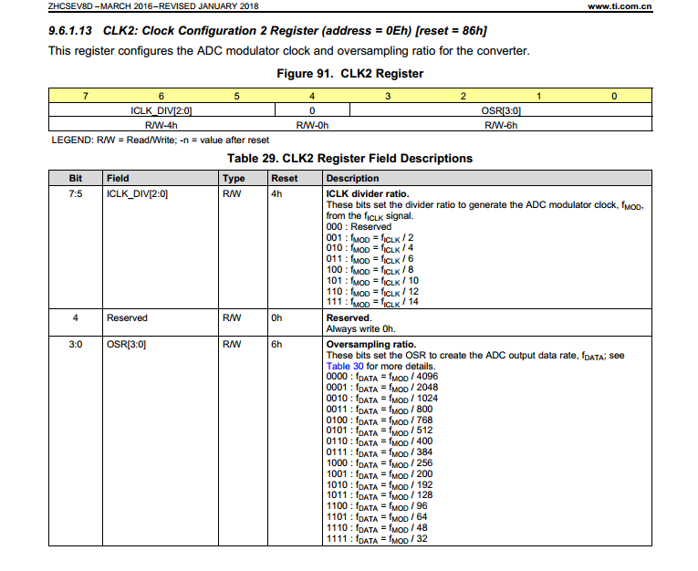
the value of the register -CLK2 is 0x86.
according to the datasheet, the default value of CLK1 is 0x08 and the default value of CLK2 is 0x86. so , the value of read the CLK1 register is error, but the another is OK. why?
the register map as follows: