This thread has been locked.

If you have a related question, please click the "Ask a related question" button in the top right corner. The newly created question will be automatically linked to this question.

ADS124S06: Gain Calibration

Part Number: ADS124S06

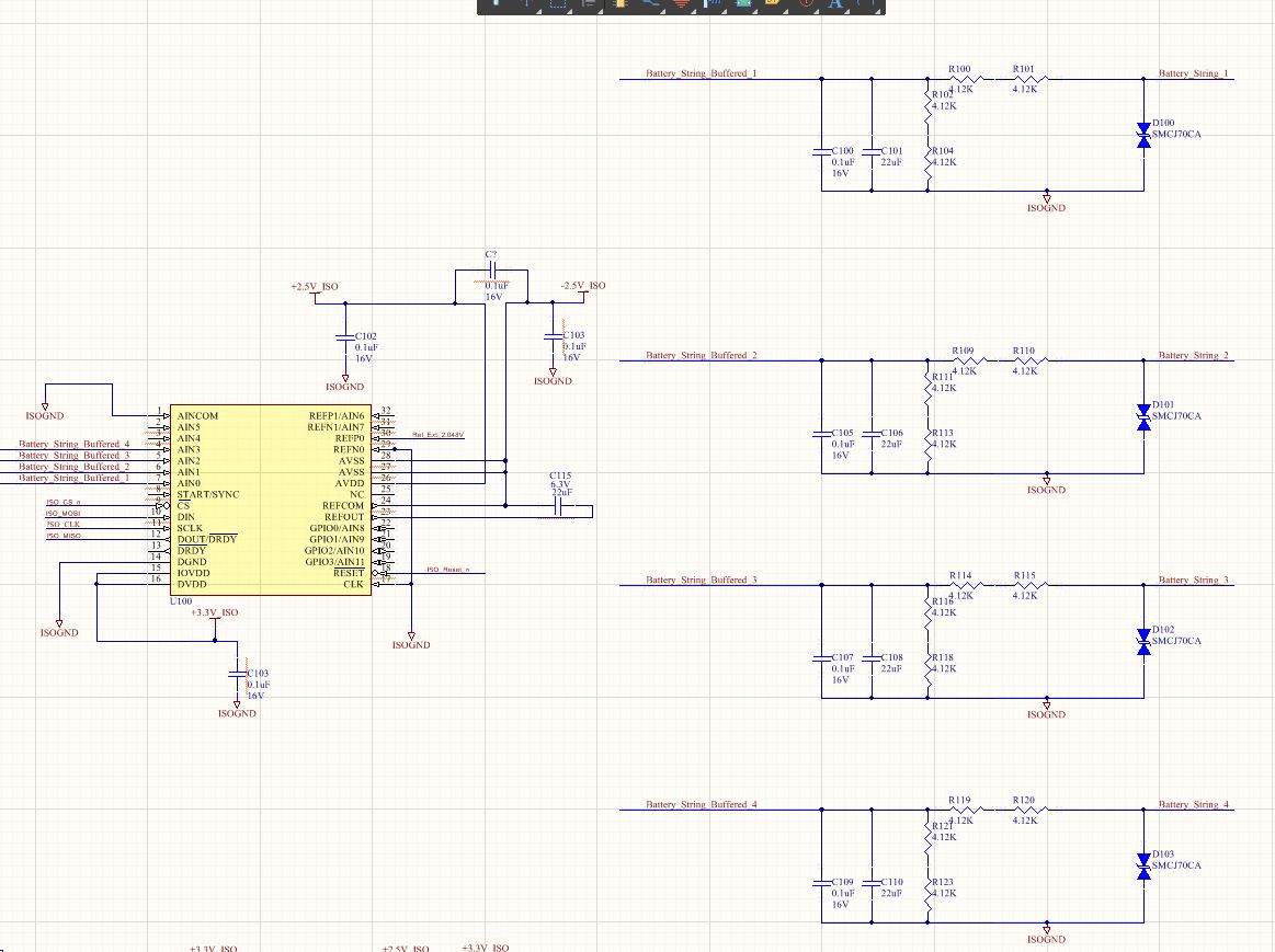
We have the following  system

-Bipolar +/-2.5V supply

-internal 2.5V supply

Q1) Is it possible to run the Gain calibration in this system? If so do we need to bypass the PGA during the calibration process?

With a -Bipolar +/-2.5V supply the PGA output is limited to AVDD-0.15V's. Gain calibration requires the full reference voltage to be applied to AINP, which is 2.5V's

However the output of the PGA is limited to AVDD-.15V's.

Purpose of the gain calibration is to zero out the error intraduced by the restive divider that feeds the ADC.

Q2) Once the Gain calibration is completed, what is the effect of changing the PGA setting?

  • Hi Burak,

    I'm not entirely sure I understand your end goal.  Can you share your schematic? 

    If you have an analog input that traverses the full range of the analog supply you cannot use the PGA.  You will have linearity issues near the supply rails and this cannot be calibrated out.  This case would require the PGA bypassed.  You will still have linearity issues if the analog input exceeds the supply by more than 50mV.

    If I understand correctly, you want to adjusts the gain based on an input voltage from the voltage divider.  This sounds like you are trying to avoid precision resistors.  If that is the case, the resistor drift can be an issue.  Keep in mind that the temperature coefficient may cause a significant error.

    If you want to use the PGA, then I would suggest that the resistor divider be adjusted so that the input is always equal to or less than AVDD-0.15V.

    Regarding question 2, the ADS124S06 has factory trimmed calibration for each gain setting.  If you change the gain, the calibration register contents will change.  You would need to save the FSCAL register contents first, and then restore as needed.

    Best regards,

    Bob B

  • "If you want to use the PGA, then I would suggest that the resistor divider be adjusted so that the input is always equal to or less than AVDD-0.15V."

    a) Does that mean with a +/-2.5V supply internal reference cant be used if one wants to perform gain calibration ?

    b) Can one bypass the PGA and perform gain calibration with +/-2.5V supply and internal reference?

    c) Does the gain calibration need to be performed for each channel? One will need  to manage  the calibration coefficients for each channel.

    d) Is the FSC default settings different for each channel as well as each PGA setting?

  • Hi Burak,

    I still don't know detail on what you are trying to calibrate.  Let me use an example where I want to measure a +/-20V input voltage using the ADS124S06.  Using an analog supply of +/- 2.5V, and the internal reference (also 2.5V).  The maximum input voltage that I can apply to the analog inputs is 2.5V and 2.5V is 1/8 the total input voltage. So I would need to create a voltage divider where 1/8 of the voltage is dropped across the resistor I wish to measure.  If I could have any value I wanted, I might pick 7k and 1k Ohm resistors and I would measure across the 1k.  If my resistors were 0.1% tolerant, I might have a situation where the 7k resistor is -0.1% (6993 Ohms) an the 1k resistor +0.1% (1001 Ohms).  The voltage divider in this case would have a voltage across the 1k as Vin(1.001k/(1.001k + 6.993k).  For a 20V input, the voltage across the resistor is now 2.5044V (instead of the desired 2.5V).  I would like to run the SYGCAL so that at a full-scale input of my system (which is 20V) I have a compensated response so that my calculations are still using a value of 2.5V as the reference, but I get an adjusted value due to the skew in the input voltage.  In other words, I want to see 0x7FFFFF for the full-scale reading in the output code.

    This higher than expected input voltage will be ok when using the PGA disabled as I have not exceeded 50mV above the AVDD positive supply rail (assuming that the supply it is exactly at 2.5V).  However, even though I have not exceeded the absolute maximum input to the device, I will have an error if I enable the PGA.  The calibration will take place, but instead of calibrating the input voltage to the PGA, I will actually be calibrating to the output voltage of the PGA.  As the PGA is operating in a non-linear region I will also have compounded the error.

    If instead I use a resistor that is slightly lower than 1k, I can avoid the over voltage input condition.  Now, this type of calibration is using the SYGCAL.  This calibration can also be accomplished using a point-slope method where the calibration gain slope is externally determined where y = mx + b.

    See my remaining responses below.

    Best regards,

    Bob B

    burak balkuv said:

    "If you want to use the PGA, then I would suggest that the resistor divider be adjusted so that the input is always equal to or less than AVDD-0.15V."

    a) Does that mean with a +/-2.5V supply internal reference cant be used if one wants to perform gain calibration ? [Bob]  You can still use the internal reference, you just can't over-range the PGA.

    b) Can one bypass the PGA and perform gain calibration with +/-2.5V supply and internal reference? [Bob] See my example above.

    c) Does the gain calibration need to be performed for each channel? One will need  to manage  the calibration coefficients for each channel. [Bob] This is difficult to answer without seeing your schematic.  First you have to determine if calibration is even necessary in the first place.  If it is required and if you had 4 different input with 4 different voltage dividers, then calibration of each input channel may need to be required.  Before doing all this effort you need to determine if you really need to calibrate or if the error is acceptable.

    d) Is the FSC default settings different for each channel as well as each PGA setting? [Bob] The factory calibration is not channel specific and will only change value when changing the PGA gain.

  • Thank you!

    Here is the schematic, resistor values are off. The scaling will be 24:1. Unfortunately calibration will be required.

    One final question on

    When using an external reference does the REFN0 get connected to AVSS which is -2.5V or midpoint  (AVSS+AVDD)/2

  • Hi Burak,

    A couple of things schematically.  You need to have a 330nF cap connected between AVDD and AVSS.  Also, if you use large resistances in the input path the 22uF caps will take a significant amount of time to settle to 1/2 LSB, so you might want to consider this moving forward.

    As your maximum input voltage is +/- 2.048V (based on external reference input) then you can safely use the PGA enabled at a gain of 1 with the single-ended measurements.

    The external reference input can have a range that is within the range of the supply.  This information is in section 7.3 of the ADS124S06 datasheet on page 8.  So you can connect REFN0 to ISOGND or AVSS.  If you connect to AVSS then you should disable the negative reference buffer.  Connecting to ISOGND probably makes the most sense and you can enable both the positive and negative reference buffers.

    For the calibration, each input channel should be calibrated using SYGCAL.  Before issuing SYGCAL, issue the SFOCAL first. Following the SYGCAL, store the settings in your micro or some other flash to be able to restore them when changing channels.  After the SYGCAL the new gain calibration values will be in the three FSCAL registers.  Store these settings, and move to the next input repeating the process.

    When muxing through the channels, restore the FSCAL registers for that channel before starting the conversion.

    Best regards,

    Bob B