Part Number: ADS54J42EVM
Hi TI Experts,
I've been trying to interface the ADS54J42 EVM with the Intel Arria 10 FPGA Development Board. I have them connected via FMC. Thus far, I've been unsuccessful.
To clarify, my JESD204B module on the FPGA is configured as a receiver with subclass 1, 2500 Mbps data rate, Soft PCS enabled, 62.5 MHz Reference Clock, LMFS = 8224, K = 32, N = 14, N’ = 16, and scrambling enabled (though I think this should not affect the link sequence).
I am using Intel's Signal Tap to capture the signals going to/coming from the interface. Here are some screenshots:
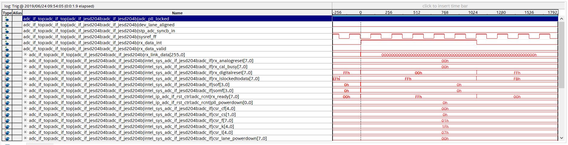
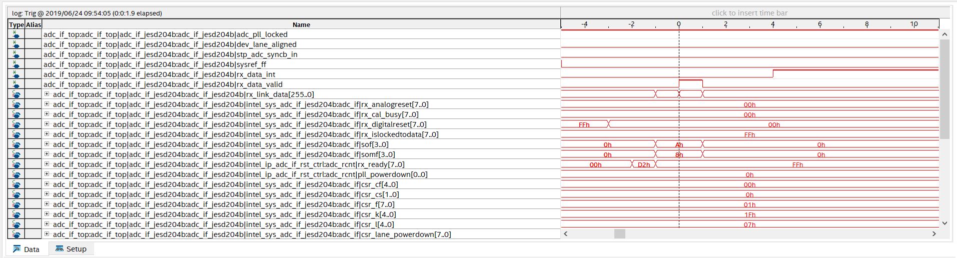
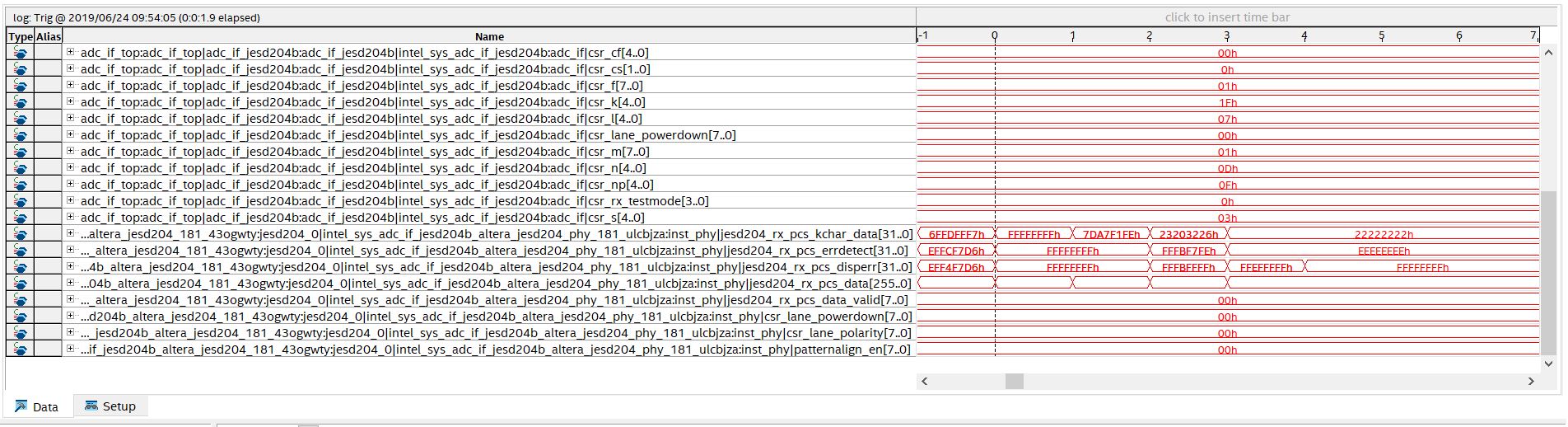
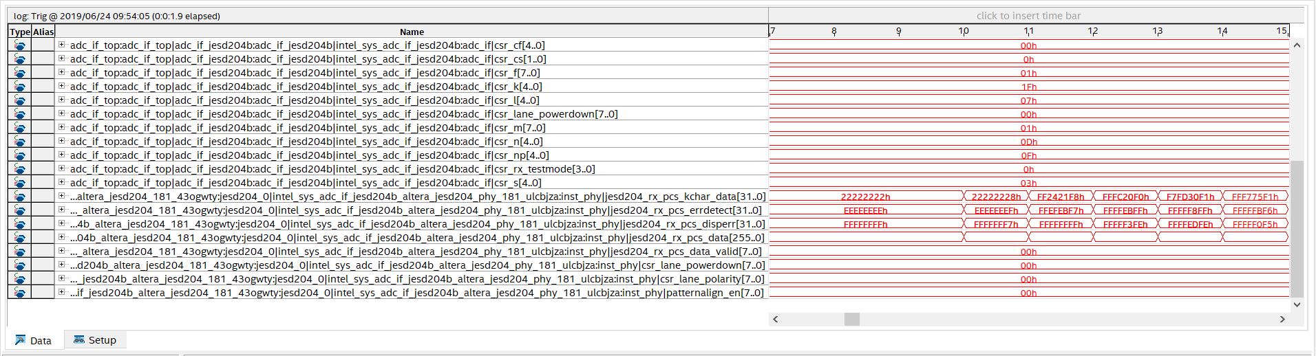
rx_islockedtodata is input to my reset controller from the JESD IF. It goes from some value (0xEF in the screenshots) to 0xFF. After some time, the rx_digitalreset (input to JESD IF from reset controller) goes from 0xFF to 0x00, and rx_ready (input to JESD IF from reset controller) goes from some value (0xD2 in the screenshots) to 0xFF. I think this is to indicate that all lanes are ready.
At this point, rx_data_valid pulses, and then the interrupt signal rx_data_int is asserted for some time. Once it is deasserted, the digital reset signal is again 0xFF, and the rx_islockedtodata goes back to some non-0xFF value (0xFB in the screenshots).
From my simulations, I expect that after this reset sequence:
- rx_is_lockedtodata 0x00 -> 0xFF
- rx_digitalreset 0xFF -> 0x00 & rx_ready 0x00 -> 0xFF
the adc_syncb_in signal will be asserted, followed by the dev_lane_aligned. After this, rx_data_valid will be asserted with valid data from the serial data pins. The interrupt signal is not asserted.
I've attached the cfg files given to me for this link up test with the ADC EVM board. The instructions are to follow this procedure for a 500 MHz external clock input to the LMK:
1. Launch ADC54Jxx EVM GUI
2. Confirm that the USB Status LED on the GUI is on
3. Load LMK_Config_External_Clock.cfg in the "Low Level View" Tab
4. Confirm that D1 & D2 LEDs do not light
5. Press SW1 for ADC Reset
6. Load ADS54J40_LMF_8224_K32.cfg in the Low Level View Tab
I'm stumped and was hoping for your insight. Here are some of my questions:
1. Is the ADC configured correctly given the config file attached?
2. Is the LMK clock source configured correctly given the config file attached? The expected clock outputs are 62.5 MHz for the device clock & 3.90625 MHz for the system reference clock for an external 500 MHz reference clock input to the J6 LMK_CLKIN port.
3. Do I have to desolder the shunt component in SJP2 since I'm using an external clock source?
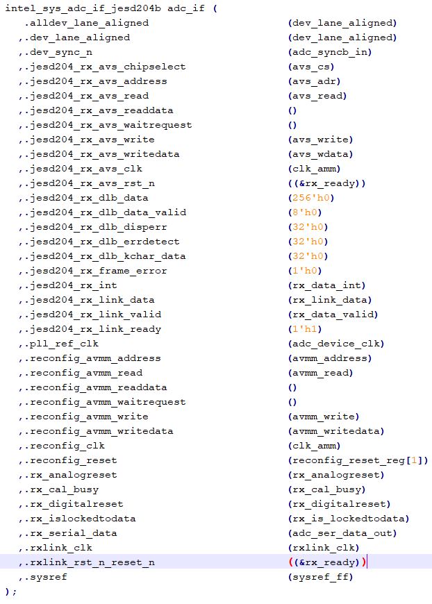
4. Should I be using the CLK_LAO_0 signal? Currently I use the FPGA_JESD_CLK at my 62.5 MHz device clock. This is input to the JESD Interface module as a pll_ref_clk signal. My rxlink_clk is also a 62.5 MHz clock, which is the output of another PLL which uses the FPGA_JESD_CLK as reference to output the 62.5 MHz rxlink_clk (as well as some other clocks for the system).
Apologies for the long post, and thank you in advance for any insight.
Regards,
Abdul