Hi,
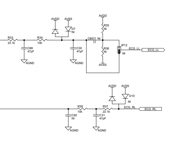
I'm developing the schematics for my custom board using the ADS1298R. I am trying to connect the channel circuits and I came across the following circuit on the PDK schematics. (Which I am referring to as per my tests of the software). I noticed that there is a diode circuit with AVDD on one side and a diode circuit with AVSS (which is not imposed). What is the purpose of this diode circuit? From my understanding, the LA/RA signal is going to be a small voltage; what is the purpose of the diodes at the end of each lead signal?
Thanks.