This thread has been locked.

If you have a related question, please click the "Ask a related question" button in the top right corner. The newly created question will be automatically linked to this question.

ADS8588S: Issue with Data Read / Convert , ADC transfers wrong values

Part Number: ADS8588S

Dear All,

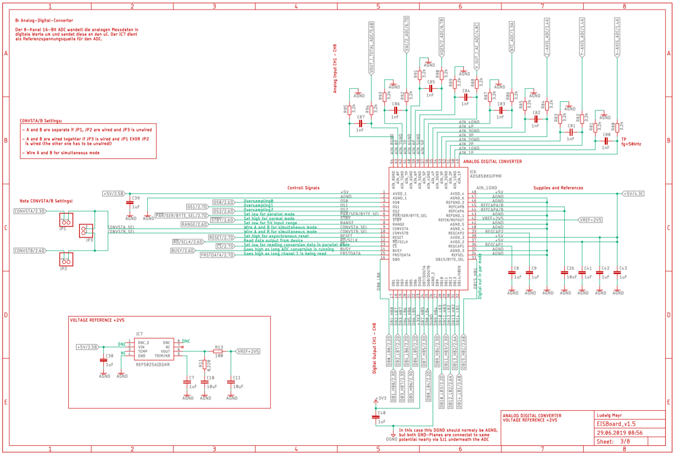
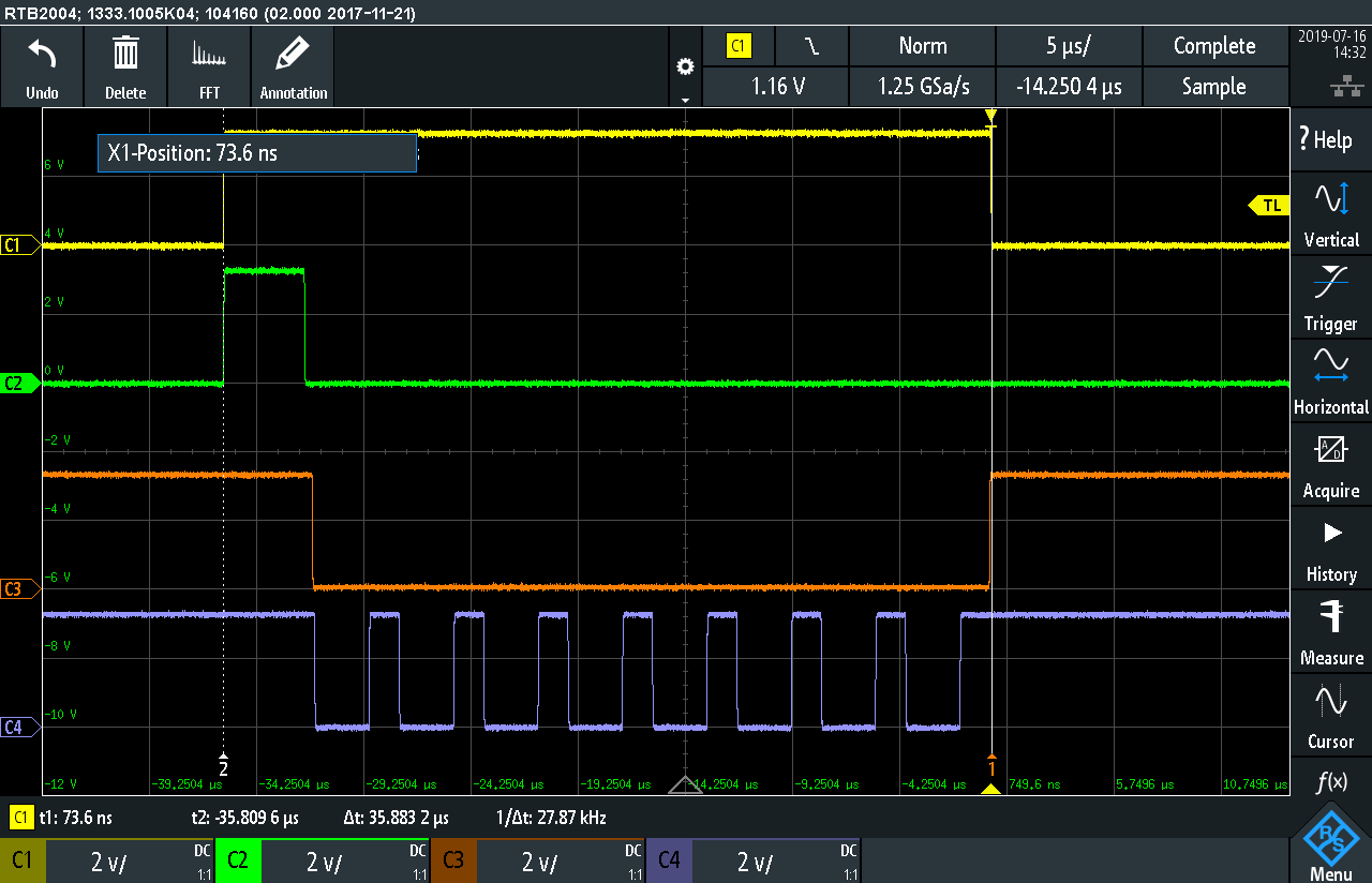
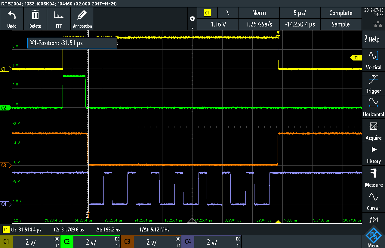
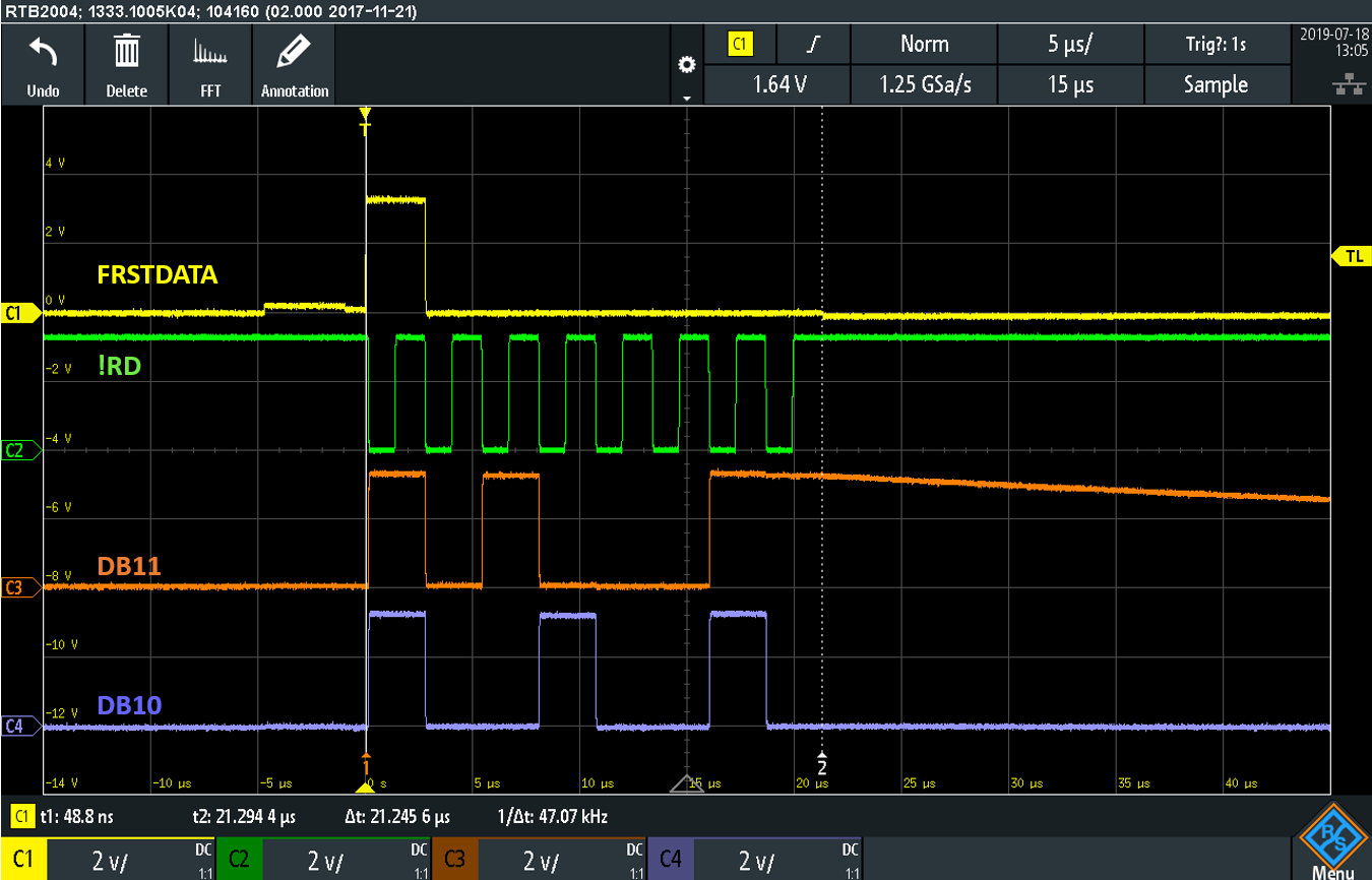
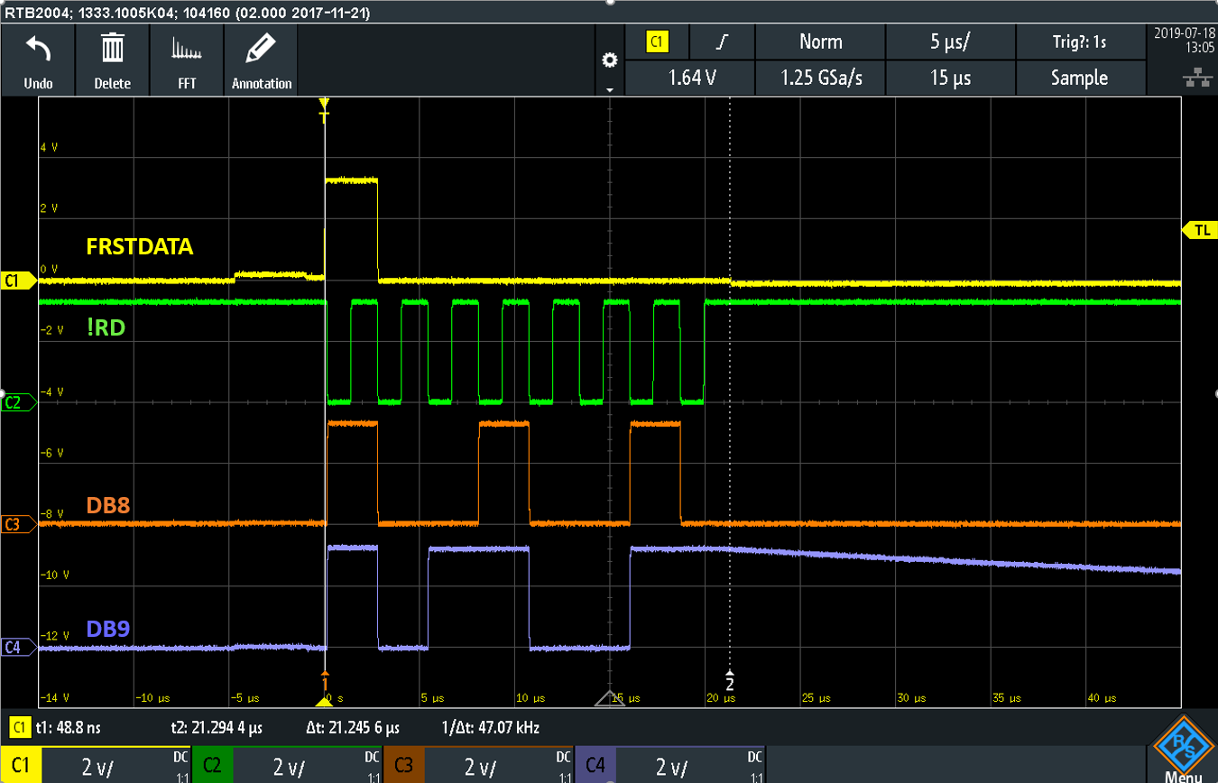
There's an issue during Data Read / Convert so the ADC sends out wrong digital values.

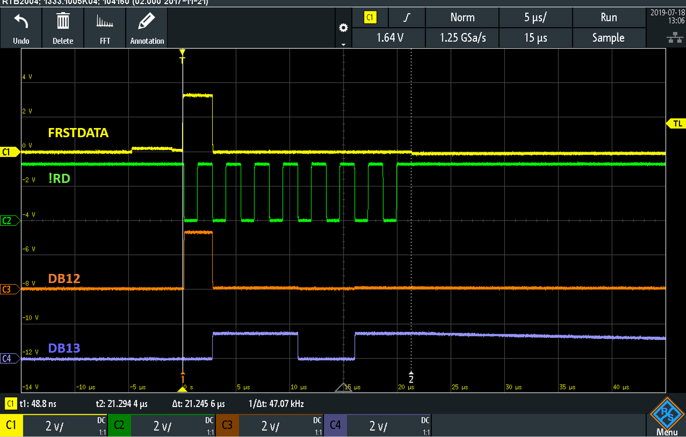
The ADC operates in 5 V-Range, simultaneous sampling on all input channels, parallel data read, external 2,5V-REF, no oversampling.

From Analog-Input-Range 0 V to 1,24 V the converted voltages are correct.

From 1,25 V to 2,4 V the digital voltages are higher by an offset of +2,5 V as they should be.

From 2,5 V to 3,75 V the digital voltages are higher by an offset of +1,25 V as they should be.

From 3,75 V to 5 V (PSR) the voltages are correct again.

I've checked the Bits [DB15:0] with a logic analyzer, so my interpretation of the values has to be correct.

Do you have any Idea why the ADC is acting like that?

I am able to send you the layout, the schematic and the implemented C code from uC which is controlling the ADC if there is any contact.

Thank you in advance.
Regards
Luke

  • Hello,

    would you please share the scope shot/logic analyzer shots showing this behavior? And also the schematic, I would like to verify the input is being driven correctly.

    It looks like there is an issue reading the MSB. In the scope shot, include the digital communications to make sure the timing is correct.

    If you look at the correct expected input and what you are seeing, there is a pattern.

    Input             Correct                                                  Customer

    1.24              0011 1111 0111 1101                     0011 1111 0111 1101

    1.25              0011 0011 0011 0011                     1100 0000 0000 0000

    2            0110 0110 0110 0110                     1110 0110 0110 0110

    2.4                0111 1010 1110 0001                     1111 1010 1110 0001

    2.5                1000 0000 0000 0000                     1100 0000 0000 0000

    3                   1001 1001 1001 1010                     1101 1001 1001 1010

    3.75              1100 0000 0000 0000                     1100 0000 0000 0000

    Regards

    Cynthia

  • Hello Cynthia,

    Thanks for your answer!

    Here you can see the schematic:

    - Only the REFSEL-Pin is hard-wired to GND

    - OS[2:0] are pulled to low via uC (no oversampling)

    - !PAR/SER/BYTE_SEL is pulled to low via uC (parallel data read)

    - !STBY is pulled up via uC (always on)

    - RANGE is pulled low via uC for 5V-Range

    - CONVSTA and CONVSTB are tied together and are code-controlled

    - !RD and !CS are seperate and code-controlled

    - RESET is code-controlled

    For the uC i'm using a STM32F446, coding is in C with ARM Keil Compiler. I've attached the Source-Code at the end  (ADC-Functions are marked bold).

    There's an scope shot of the control timings (not in picture: CONVSTA/B-Signal: it goes on high immediately befor BUSY goes high, and goes back to low if !CS is going back to high):

    Here's an example for some value i get:

      Analog SOLL Digital DEZ Analog IST Analog KOR
    CH1 1,654 27218 4,153137207 1,653
    CH2 1,665 27290 4,164123535 1,664
    CH3 1,659 27246 4,157409668 1,657
    CH4 1,388 25834 3,941955566 1,442
    CH5 0 2 0,000305176 0
    CH6 0,005 22 0,003356934 0,003
    CH7 0,212 2098 0,320129395 0,32
    CH8 1,651 27174 4,14642334 1,646

    I can send you logic analyzer shot on this tomorrow.

    Thank you very much so far! I really appreciate your help!

    Regards

    Luke

    Source Code:

    /* Includes ------------------------------------------------------------------*/
    #include "main.h"

    /* Private includes ----------------------------------------------------------*/
    /* USER CODE BEGIN Includes */
    #include <stdbool.h>
    /* USER CODE END Includes */

    /* Private typedef -----------------------------------------------------------*/
    /* USER CODE BEGIN PTD */

    /* USER CODE END PTD */

    /* Private define ------------------------------------------------------------*/
    /* USER CODE BEGIN PD */

    /* USER CODE END PD */

    /* Private macro -------------------------------------------------------------*/
    /* USER CODE BEGIN PM */

    /* USER CODE END PM */

    /* Private variables ---------------------------------------------------------*/
    CAN_HandleTypeDef hcan1;
    DAC_HandleTypeDef hdac;

    /* USER CODE BEGIN PV */
    // CAN variables
    CAN_TxHeaderTypeDef TxHeader;
    CAN_RxHeaderTypeDef RxHeader;
    uint8_t TxData[8];
    uint8_t RxData[8];
    uint32_t TxMailbox;

    // ADC variables
    uint16_t usi_adc_global[8];
    bool tempVar_global = true;
    /* USER CODE END PV */

    /* Private function prototypes -----------------------------------------------*/
    void SystemClock_Config(void);
    static void MX_GPIO_Init(void);
    static void MX_DAC_Init(void);
    static void MX_CAN1_Init(void);
    /* USER CODE BEGIN PFP */
    void _initAdc(void);
    void _resetAdc(void);
    void _startAdcConv(void);
    void _ISR_adcFinished(void);
    void _SysDelay(void);
    /* USER CODE END PFP */

    /* Private user code ---------------------------------------------------------*/
    /* USER CODE BEGIN 0 */

    /* USER CODE END 0 */

    /**
      * @brief  The application entry point.
      * @retval int
      */
    int main(void)
    {
      /* USER CODE BEGIN 1 */

      /* USER CODE END 1 */
     

      /* MCU Configuration--------------------------------------------------------*/

      /* Reset of all peripherals, Initializes the Flash interface and the Systick. */
      HAL_Init();

      /* USER CODE BEGIN Init */

      /* USER CODE END Init */

      /* Configure the system clock */
      SystemClock_Config();

      /* USER CODE BEGIN SysInit */

      /* USER CODE END SysInit */

      /* Initialize all configured peripherals */
      MX_GPIO_Init();
      MX_DAC_Init();
      MX_CAN1_Init();
      /* USER CODE BEGIN 2 */
        HAL_GPIO_WritePin(GPIOB, RANGE_Pin, GPIO_PIN_RESET);
        HAL_Delay(1000);                                                                                // debug-delay
        HAL_GPIO_WritePin(GPIOC, LED1_Pin, GPIO_PIN_SET);                // set Green LED to show up SystemInit
        _resetAdc();                                                            
      /* USER CODE END 2 */

      /* Infinite loop */
      /* USER CODE BEGIN WHILE */
      while (1)
      {
        /* USER CODE END WHILE */

        /* USER CODE BEGIN 3 */
            if ((HAL_GPIO_ReadPin(GPIOC, B1_Pin) == GPIO_PIN_RESET) && tempVar_global)            // wait for UserPushButton is pressed
            {
                _startAdcConv();                                                                                                                            // then start ADC
                tempVar_global = false;
            }
            else if ((HAL_GPIO_ReadPin(GPIOC, B1_Pin) == GPIO_PIN_SET))
            {
                tempVar_global = true;
            }
        }
      /* USER CODE END 3 */
    }

    /**
      * @brief System Clock Configuration
      * @retval None
      */
    void SystemClock_Config(void)
    {
      RCC_OscInitTypeDef RCC_OscInitStruct = {0};
      RCC_ClkInitTypeDef RCC_ClkInitStruct = {0};

      /** Configure the main internal regulator output voltage
      */
      __HAL_RCC_PWR_CLK_ENABLE();
      __HAL_PWR_VOLTAGESCALING_CONFIG(PWR_REGULATOR_VOLTAGE_SCALE1);
      /** Initializes the CPU, AHB and APB busses clocks
      */
      RCC_OscInitStruct.OscillatorType = RCC_OSCILLATORTYPE_HSI;
      RCC_OscInitStruct.HSIState = RCC_HSI_ON;
      RCC_OscInitStruct.HSICalibrationValue = RCC_HSICALIBRATION_DEFAULT;
      RCC_OscInitStruct.PLL.PLLState = RCC_PLL_ON;
      RCC_OscInitStruct.PLL.PLLSource = RCC_PLLSOURCE_HSI;
      RCC_OscInitStruct.PLL.PLLM = 8;
      RCC_OscInitStruct.PLL.PLLN = 180;
      RCC_OscInitStruct.PLL.PLLP = RCC_PLLP_DIV2;
      RCC_OscInitStruct.PLL.PLLQ = 2;
      RCC_OscInitStruct.PLL.PLLR = 2;
      if (HAL_RCC_OscConfig(&RCC_OscInitStruct) != HAL_OK)
      {
        Error_Handler();
      }
      /** Activate the Over-Drive mode
      */
      if (HAL_PWREx_EnableOverDrive() != HAL_OK)
      {
        Error_Handler();
      }
      /** Initializes the CPU, AHB and APB busses clocks
      */
      RCC_ClkInitStruct.ClockType = RCC_CLOCKTYPE_HCLK|RCC_CLOCKTYPE_SYSCLK
                                  |RCC_CLOCKTYPE_PCLK1|RCC_CLOCKTYPE_PCLK2;
      RCC_ClkInitStruct.SYSCLKSource = RCC_SYSCLKSOURCE_PLLCLK;
      RCC_ClkInitStruct.AHBCLKDivider = RCC_SYSCLK_DIV1;
      RCC_ClkInitStruct.APB1CLKDivider = RCC_HCLK_DIV4;
      RCC_ClkInitStruct.APB2CLKDivider = RCC_HCLK_DIV2;

      if (HAL_RCC_ClockConfig(&RCC_ClkInitStruct, FLASH_LATENCY_5) != HAL_OK)
      {
        Error_Handler();
      }
    }

    /**
      * @brief CAN1 Initialization Function
      * @param None
      * @retval None
      */
    static void MX_CAN1_Init(void)
    {

      /* USER CODE BEGIN CAN1_Init 0 */

      /* USER CODE END CAN1_Init 0 */

      /* USER CODE BEGIN CAN1_Init 1 */

      /* USER CODE END CAN1_Init 1 */
      hcan1.Instance = CAN1;
      hcan1.Init.Prescaler = 10;
      hcan1.Init.Mode = CAN_MODE_NORMAL;
      hcan1.Init.SyncJumpWidth = CAN_SJW_1TQ;
      hcan1.Init.TimeSeg1 = CAN_BS1_6TQ;
      hcan1.Init.TimeSeg2 = CAN_BS2_2TQ;
      hcan1.Init.TimeTriggeredMode = DISABLE;
      hcan1.Init.AutoBusOff = DISABLE;
      hcan1.Init.AutoWakeUp = DISABLE;
      hcan1.Init.AutoRetransmission = DISABLE;
      hcan1.Init.ReceiveFifoLocked = DISABLE;
      hcan1.Init.TransmitFifoPriority = DISABLE;
      if (HAL_CAN_Init(&hcan1) != HAL_OK)
      {
        Error_Handler();
      }
      /* USER CODE BEGIN CAN1_Init 2 */

      /* USER CODE END CAN1_Init 2 */

    }

    /**
      * @brief DAC Initialization Function
      * @param None
      * @retval None
      */
    static void MX_DAC_Init(void)
    {

      /* USER CODE BEGIN DAC_Init 0 */

      /* USER CODE END DAC_Init 0 */

      DAC_ChannelConfTypeDef sConfig = {0};

      /* USER CODE BEGIN DAC_Init 1 */

      /* USER CODE END DAC_Init 1 */
      /** DAC Initialization
      */
      hdac.Instance = DAC;
      if (HAL_DAC_Init(&hdac) != HAL_OK)
      {
        Error_Handler();
      }
      /** DAC channel OUT1 config
      */
      sConfig.DAC_Trigger = DAC_TRIGGER_NONE;
      sConfig.DAC_OutputBuffer = DAC_OUTPUTBUFFER_ENABLE;
      if (HAL_DAC_ConfigChannel(&hdac, &sConfig, DAC_CHANNEL_1) != HAL_OK)
      {
        Error_Handler();
      }
      /** DAC channel OUT2 config
      */
      if (HAL_DAC_ConfigChannel(&hdac, &sConfig, DAC_CHANNEL_2) != HAL_OK)
      {
        Error_Handler();
      }
      /* USER CODE BEGIN DAC_Init 2 */

      /* USER CODE END DAC_Init 2 */

    }

    /**
      * @brief GPIO Initialization Function
      * @param None
      * @retval None
      */
    static void MX_GPIO_Init(void)
    {
      GPIO_InitTypeDef GPIO_InitStruct = {0};

      /* GPIO Ports Clock Enable */
      __HAL_RCC_GPIOC_CLK_ENABLE();
      __HAL_RCC_GPIOH_CLK_ENABLE();
      __HAL_RCC_GPIOA_CLK_ENABLE();
      __HAL_RCC_GPIOB_CLK_ENABLE();
      __HAL_RCC_GPIOD_CLK_ENABLE();

      /*Configure GPIO pin Output Level */
      HAL_GPIO_WritePin(GPIOA, CAN1_EN_Pin|RD_SCLK_Pin, GPIO_PIN_SET);

      /*Configure GPIO pin Output Level */
      HAL_GPIO_WritePin(GPIOC, CONVSTB_Pin|CONVSTA_Pin|LED1_Pin|LED2_Pin, GPIO_PIN_RESET);

      /*Configure GPIO pin Output Level */
      HAL_GPIO_WritePin(CS_GPIO_Port, CS_Pin, GPIO_PIN_SET);

      /*Configure GPIO pin Output Level */
      HAL_GPIO_WritePin(GPIOB, PAR_SER_BYTE_SEL_Pin|RANGE_Pin|OS0_Pin|OS1_Pin
                              |OS2_Pin|DELAY_Pin, GPIO_PIN_RESET);

      /*Configure GPIO pin Output Level */
      HAL_GPIO_WritePin(STBY_GPIO_Port, STBY_Pin, GPIO_PIN_SET);

      /*Configure GPIO pin Output Level */
      HAL_GPIO_WritePin(GPIOA, RESET_Pin|LED3_Pin, GPIO_PIN_RESET);

      /*Configure GPIO pins : B1_Pin DB15_HB1_Pin DB14_LB1_Pin BUSY_Pin
                               DB9_HB4_Pin FRSTDATA_Pin DB12_LB2_Pin */
      GPIO_InitStruct.Pin = B1_Pin|DB15_HB1_Pin|DB14_LB1_Pin|BUSY_Pin
                              |DB9_HB4_Pin|FRSTDATA_Pin|DB12_LB2_Pin;
      GPIO_InitStruct.Mode = GPIO_MODE_INPUT;
      GPIO_InitStruct.Pull = GPIO_NOPULL;
      HAL_GPIO_Init(GPIOC, &GPIO_InitStruct);

      /*Configure GPIO pins : DB1_HB8_Pin DB0_LB8_Pin DB11_HB3_Pin DB7_HB5_Pin
                               DB8_LB4_Pin DB2_LB7_Pin */
      GPIO_InitStruct.Pin = DB1_HB8_Pin|DB0_LB8_Pin|DB11_HB3_Pin|DB7_HB5_Pin
                              |DB8_LB4_Pin|DB2_LB7_Pin;
      GPIO_InitStruct.Mode = GPIO_MODE_INPUT;
      GPIO_InitStruct.Pull = GPIO_NOPULL;
      HAL_GPIO_Init(GPIOA, &GPIO_InitStruct);

      /*Configure GPIO pins : CAN1_EN_Pin RD_SCLK_Pin */
      GPIO_InitStruct.Pin = CAN1_EN_Pin|RD_SCLK_Pin;
      GPIO_InitStruct.Mode = GPIO_MODE_OUTPUT_PP;
      GPIO_InitStruct.Pull = GPIO_PULLUP;
      GPIO_InitStruct.Speed = GPIO_SPEED_FREQ_LOW;
      HAL_GPIO_Init(GPIOA, &GPIO_InitStruct);

      /*Configure GPIO pins : CONVSTB_Pin CONVSTA_Pin LED1_Pin LED2_Pin */
      GPIO_InitStruct.Pin = CONVSTB_Pin|CONVSTA_Pin|LED1_Pin|LED2_Pin;
      GPIO_InitStruct.Mode = GPIO_MODE_OUTPUT_PP;
      GPIO_InitStruct.Pull = GPIO_NOPULL;
      GPIO_InitStruct.Speed = GPIO_SPEED_FREQ_LOW;
      HAL_GPIO_Init(GPIOC, &GPIO_InitStruct);

      /*Configure GPIO pin : CS_Pin */
      GPIO_InitStruct.Pin = CS_Pin;
      GPIO_InitStruct.Mode = GPIO_MODE_OUTPUT_PP;
      GPIO_InitStruct.Pull = GPIO_PULLUP;
      GPIO_InitStruct.Speed = GPIO_SPEED_FREQ_LOW;
      HAL_GPIO_Init(CS_GPIO_Port, &GPIO_InitStruct);

      /*Configure GPIO pins : PAR_SER_BYTE_SEL_Pin OS0_Pin OS1_Pin OS2_Pin */
      GPIO_InitStruct.Pin = PAR_SER_BYTE_SEL_Pin|OS0_Pin|OS1_Pin|OS2_Pin;
      GPIO_InitStruct.Mode = GPIO_MODE_OUTPUT_PP;
      GPIO_InitStruct.Pull = GPIO_PULLDOWN;
      GPIO_InitStruct.Speed = GPIO_SPEED_FREQ_LOW;
      HAL_GPIO_Init(GPIOB, &GPIO_InitStruct);

      /*Configure GPIO pin : STBY_Pin */
      GPIO_InitStruct.Pin = STBY_Pin;
      GPIO_InitStruct.Mode = GPIO_MODE_OUTPUT_PP;
      GPIO_InitStruct.Pull = GPIO_PULLUP;
      GPIO_InitStruct.Speed = GPIO_SPEED_FREQ_LOW;
      HAL_GPIO_Init(STBY_GPIO_Port, &GPIO_InitStruct);

      /*Configure GPIO pins : DB6_LB5_Pin DB3_HB7_Pin DB5_HB6_Pin DB4_LB6_Pin
                               DB10_LB3_Pin */
      GPIO_InitStruct.Pin = DB6_LB5_Pin|DB3_HB7_Pin|DB5_HB6_Pin|DB4_LB6_Pin
                              |DB10_LB3_Pin;
      GPIO_InitStruct.Mode = GPIO_MODE_INPUT;
      GPIO_InitStruct.Pull = GPIO_NOPULL;
      HAL_GPIO_Init(GPIOB, &GPIO_InitStruct);

      /*Configure GPIO pins : RANGE_Pin DELAY_Pin */
      GPIO_InitStruct.Pin = RANGE_Pin|DELAY_Pin;
      GPIO_InitStruct.Mode = GPIO_MODE_OUTPUT_PP;
      GPIO_InitStruct.Pull = GPIO_NOPULL;
      GPIO_InitStruct.Speed = GPIO_SPEED_FREQ_LOW;
      HAL_GPIO_Init(GPIOB, &GPIO_InitStruct);

      /*Configure GPIO pins : RESET_Pin LED3_Pin */
      GPIO_InitStruct.Pin = RESET_Pin|LED3_Pin;
      GPIO_InitStruct.Mode = GPIO_MODE_OUTPUT_PP;
      GPIO_InitStruct.Pull = GPIO_NOPULL;
      GPIO_InitStruct.Speed = GPIO_SPEED_FREQ_LOW;
      HAL_GPIO_Init(GPIOA, &GPIO_InitStruct);

      /*Configure GPIO pin : DB13_HB2_Pin */
      GPIO_InitStruct.Pin = DB13_HB2_Pin;
      GPIO_InitStruct.Mode = GPIO_MODE_INPUT;
      GPIO_InitStruct.Pull = GPIO_NOPULL;
      HAL_GPIO_Init(DB13_HB2_GPIO_Port, &GPIO_InitStruct);

    }

    /* USER CODE BEGIN 4 */


    /**
      * @brief ADC Reset Function
      * @param None
      * @retval None
      */
    void _resetAdc(void)
    {
        HAL_GPIO_WritePin(GPIOA, RESET_Pin, GPIO_PIN_SET);                // set RESET high for ADC-Reset
        HAL_Delay(1);                                                                                            // wait in RESET-State, RESET high has to be min. 50 ns
        HAL_GPIO_WritePin(GPIOA, RESET_Pin, GPIO_PIN_RESET);            // set RESET back to low
        
        HAL_Delay(1000);                                                                                    // wait for user show up and safe states
        HAL_GPIO_WritePin(GPIOC, LED2_Pin, GPIO_PIN_SET);                    // set Blue LED to show up ADC is ready after Reset
    }

    /**
      * @brief ADC Conversion Function. Starts the Conversion and goes on if Conversion is done
      * @param None
      * @retval None
      */
    void _startAdcConv(void)
    {
        HAL_GPIO_WritePin(GPIOA, LED3_Pin, GPIO_PIN_SET);                // set Red LED to show up Conversion has started
        HAL_Delay(1000);                                                                                // for debugg to show User the State
        
        HAL_GPIO_WritePin(GPIOC, CONVSTA_Pin, GPIO_PIN_SET);        // CONVSTA is tied to CONVSTB via hardware setup
        //HAL_GPIO_WritePin(GPIOC, CONVSTB_Pin, GPIO_PIN_SET);    // CONVSTB set only necessary if CONVSTB is not wired to CONVSTA
        
        _SysDelay();                                                                                        // 4 us Delay for BUSY-Hightime    (DataSheet = 3.8 us)
        _ISR_adcFinished();                                                                            // read Data after BUSY goes back to low
    }

    void _startAdcConv2(void)
    {
        HAL_GPIO_WritePin(GPIOC, CONVSTA_Pin, GPIO_PIN_SET);
        _SysDelay();
    }

    /**
      * @brief ADC DataRead Function
      * @param None
      * @retval None
      */
    void _ISR_adcFinished(void)
    {
        uint16_t usi_temp = 0;
        uint16_t usi_i = 0;

        HAL_GPIO_WritePin(GPIOC, CS_Pin, GPIO_PIN_RESET);                                // set !CS to low
            
        for (usi_i = 0; usi_i < 8; usi_i++)
        {
            usi_temp = 0;
                
            HAL_GPIO_WritePin(GPIOA, RD_SCLK_Pin, GPIO_PIN_RESET);                // Start CH1

            usi_temp |= (HAL_GPIO_ReadPin(GPIOC, DB15_HB1_Pin)) << 15;               // MSB
            usi_temp |= (HAL_GPIO_ReadPin(GPIOC, DB14_LB1_Pin)) << 14;
            usi_temp |= (HAL_GPIO_ReadPin(GPIOD, DB13_HB2_Pin)) << 13;
            usi_temp |= (HAL_GPIO_ReadPin(GPIOC, DB12_LB2_Pin)) << 12;
            usi_temp |= (HAL_GPIO_ReadPin(GPIOA, DB11_HB3_Pin)) << 11;
            usi_temp |= (HAL_GPIO_ReadPin(GPIOB, DB10_LB3_Pin)) << 10;
            usi_temp |= (HAL_GPIO_ReadPin(GPIOC, DB9_HB4_Pin)) << 9;
            usi_temp |= (HAL_GPIO_ReadPin(GPIOA, DB8_LB4_Pin)) << 8;
            usi_temp |= (HAL_GPIO_ReadPin(GPIOA, DB7_HB5_Pin)) << 7;
            usi_temp |= (HAL_GPIO_ReadPin(GPIOB, DB6_LB5_Pin)) << 6;
            usi_temp |= (HAL_GPIO_ReadPin(GPIOB, DB5_HB6_Pin)) << 5;
            usi_temp |= (HAL_GPIO_ReadPin(GPIOB, DB4_LB6_Pin)) << 4;
            usi_temp |= (HAL_GPIO_ReadPin(GPIOB, DB3_HB7_Pin)) << 3;
            usi_temp |= (HAL_GPIO_ReadPin(GPIOA, DB2_LB7_Pin)) << 2;
            usi_temp |= (HAL_GPIO_ReadPin(GPIOA, DB1_HB8_Pin)) << 1;
            usi_temp |= (HAL_GPIO_ReadPin(GPIOA, DB0_LB8_Pin)) << 0;                  // LSB

            usi_adc_global[usi_i] = usi_temp;
            HAL_GPIO_WritePin(GPIOA, RD_SCLK_Pin, GPIO_PIN_SET);                    // End CH1... next CH2... --> CH8        
        }
        HAL_GPIO_WritePin(GPIOC, CS_Pin, GPIO_PIN_SET);                                    // init !CS back to high    
        HAL_GPIO_WritePin(GPIOC, CONVSTA_Pin, GPIO_PIN_RESET);                    // init CONVSTA back to low
        
        HAL_Delay(2000);                                                                                                // debug-delay
        HAL_GPIO_WritePin(GPIOA, LED3_Pin, GPIO_PIN_RESET);                            // reset Red LED so show up that DataRead is complete
        HAL_GPIO_WritePin(GPIOC, LED2_Pin, GPIO_PIN_RESET);                            // reset BLue LED
        HAL_GPIO_WritePin(GPIOC, LED1_Pin, GPIO_PIN_SET);                                // set Green LED
    }

    /**
      * @brief  This function generates an UserDelay.
      * @retval None
      */
    void _SysDelay(void)
    {
        unsigned int usi_delay = 0;
        
        for (usi_delay = 0; usi_delay < 30; usi_delay++)                    // 28 times function call corresponds to a 4,2 us Delay in theroie
        {                                                                                                                    // in praxis there is a 4 us Delay
            HAL_GPIO_WritePin(GPIOB, DELAY_Pin, GPIO_PIN_SET);
            HAL_GPIO_WritePin(GPIOB, DELAY_Pin, GPIO_PIN_RESET);        // one SET and RESET Operation corresponds to a 150 ns Delay
        }
    }

  • I'm sorry the picture want send.

    There's an scope shot of the control timings (not in picture: CONVSTA/B-Signal: it goes on high immediately befor BUSY goes high, and goes back to low if !CS is going back to high):

  • Hello Cynthia,

    unfortunately i only have a 4 channel oscilloscope so i had to split the signals. First of all, again the control signals with timings:

    CONVSTA/B (yellow):

    BUSY (green):

    Delay BUSY falling edge to !CS falling edge (orange):

    Delay !CS falling edge to !RD falling edge (blue):

    Low Time !RD:

    High Time !RD:

    Are these timings correct? I've always put delays in the code to make sure i follow the min. requirements given from data sheet.

    The following scope shots are showing the data bits from DB15 to DB6, DB5 - DB4 are unrelevant so far i think:

    The actual analog input voltages are:

    CH1: 1,24 V

    CH2: 1,26 V

    CH3: 1,65 V

    CH4: 1,52 V

    CH5: 0 V

    CH6: 0 V

    CH7: 1,56 V

    CH8: 1,65 V

    I'm not sure from where the issue is coming from. Could be a timing-issue but also as well a wrong data interpretation / data read in C-code. There is often DB14 and DB13 set where it shouldn't be, as you already sad - there is a pattern.

    I am looking forward for your help. Thank you very much.

    Regards

    Luke

  • Dear Cynthia,


    did you already found time for this topic?

    i would really appreciate if i get any advice on that because this is really urgent for me.

    Thanks a lot!


    Kind regards


    Luke

  • I've fixed it on my own.

  • I apologize for the late response on this, but I am glad to hear that you were able to fix this

    Regards

    Cynthia