This thread has been locked.

If you have a related question, please click the "Ask a related question" button in the top right corner. The newly created question will be automatically linked to this question.

ADS1191: functionality test

Anonymous
Anonymous
Part Number: ADS1191
Other Parts Discussed in Thread: SN74LVC3G17, SN74LV1T34, ADS1292, ADS1298, ADS1294

Hello,

I have a question again...

In the following I wanted to concentrate on the ADS1191 first of all.
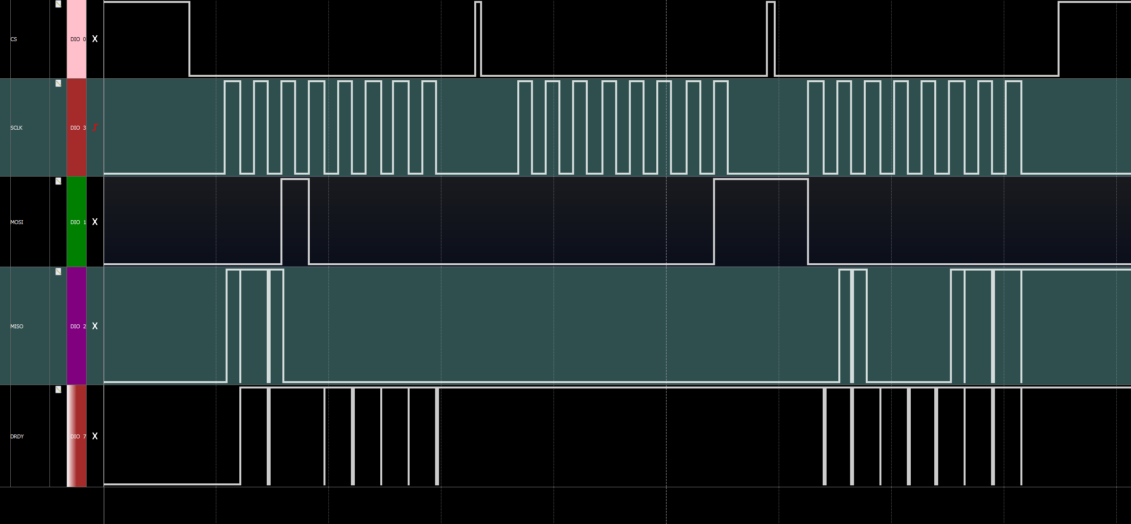
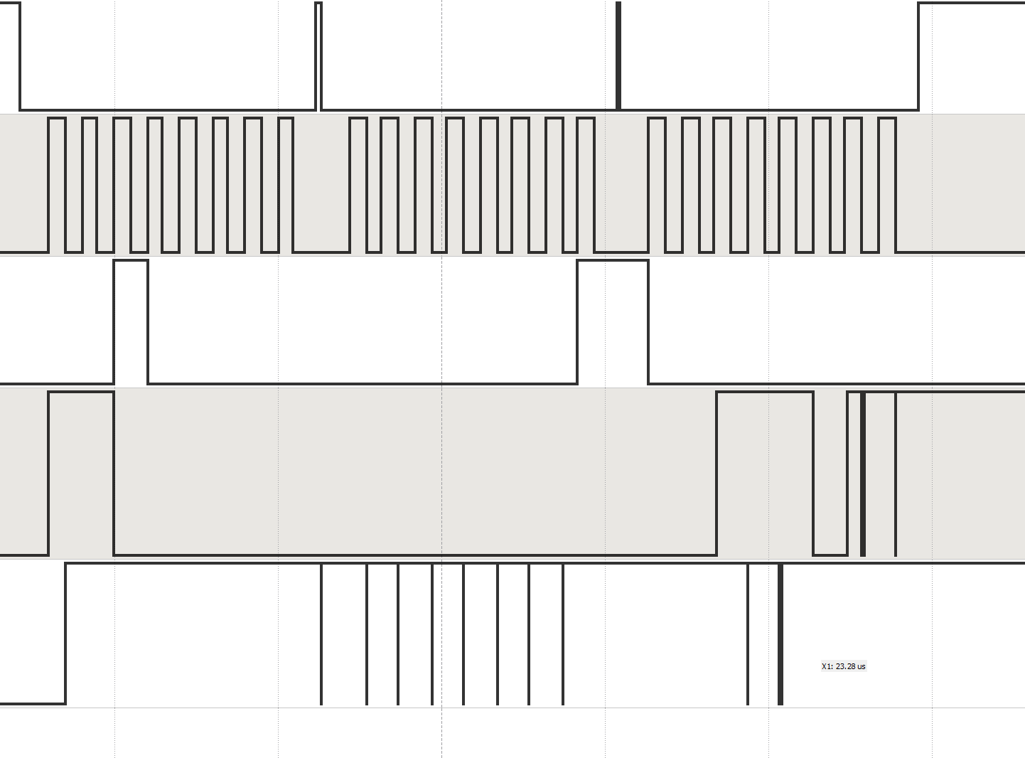
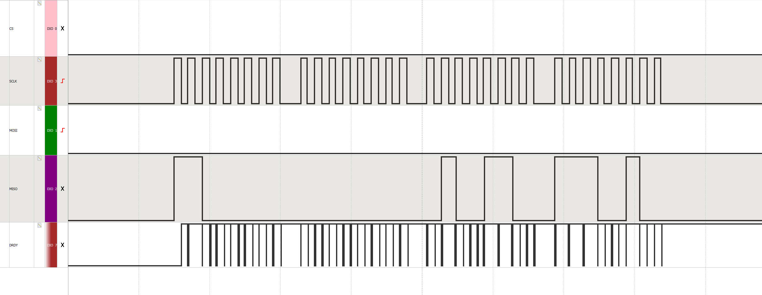
I built the following circuit: AVDD = 3.3V, DVDD = 1.8V

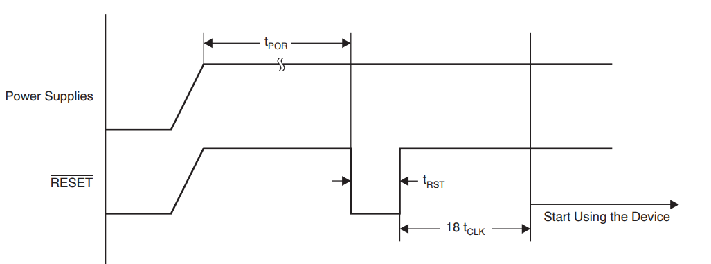
When I connect the circuit, I would expect the DRDY to start pulsing as soon as I set "Start" to High or change its status as soon as I send a command.
However, the line remains low all the time.
Can I somehow measure the full functionality of my chip or is the circuit so usable at all?

To convert my 5V digital inputs I use the SN74LVC3G17 and SN74LV1T34 as follows:

Many thanks in advance!

Hendrik

  • Hello Hendrik,

    Thank you for your post!

    How are the CLKSEL and START pins configured? Please refer to Table 9 for configuration options for the ADS1292's master clock.

    Best regards,

  • Anonymous
    0 Anonymous in reply to Ryan Andrews

    Hello Ryan,

    CLKSEL and START pins are configured as HIGH as well as the PWDN/ RESET pin. However, I am not sure about this. Should this pin be set to HIGH for Power-On and get a short reset pulse or is it okay if I set this one to high all the time as well?

    Like:

    Best regards,

    Hendrik

  • Anonymous
    0 Anonymous in reply to Anonymous

    If I try to simulate this, I can only create a pulse with a width of 3.56µs, is this too large?

    I am unsure about the exact times of t_RST and t_POR. These are multiples of t_MOD, right? The t_MOD again is either 4*tclk or 16*tclk. Depending on how CLK_DIV, the default setting is 0 if I use the internal clock with a frequency of 512kHz. 16*tclk is not a problem, 4*tclk is up to < 3.56µs and if I can assume that t_clk is in the range of 465 - 514ns.

    However, in the case of an internal clock with 512kHz and CLK_DIV == 0, the time data is specified as TBA... is it advisable to use an external oscillator with e.g. 2048kHz?

    My start algorithm works like this:

    Set RESET=== 1;
    Wait 3809µs
    Set RESET=== 0; "pulse"
    Set RESET=== 1; --> 3.56µs
    Wait 9µs
    Set START == 1;
    Set CLKSEL == 1;
    Wait 1s;
    Set RESET== 0; "puls"
    Set RESET=== 1; --> 3.56µs
    Wait 9µs

    If I use this algorithm I can at least observe a change of DRDY from HIGH to LOW.

    but then DRDY should be pulsing...

    Is it necessary to do anything with the CLK pin? For example, to pull it to GND with a pulldown resistor or something?

  • Hello Hendrick,

    The /RESET pulse is critical to the start-up routine. Please follow the POR (power-on reset) guidelines in the datasheet for timing.

    The internal delta-sigma modulator is designed to operate at 128 kHz. The master clock frequency can be either 512 kHz or 2.048 MHz, but the appropriate CLK_DIV setting must be selected to derive the 128 kHz modulator frequency (fMOD).

    The /RESET pulse must be shorter than 2^9 tMOD periods (i.e. 4 ms) in order to avoid power-down. However, it also must be held low at least 1 tMOD period, which is equal to 1 / 128 kHz or 7.1825 us. Therefore, 3.56 us is not long enough to properly reset the device.

    The CLK pin can be left floating if the device is using the internal 512-kHz master clock.

    Best regards,

  • Anonymous
    0 Anonymous in reply to Ryan Andrews

    Hello Ryan,

    I found my mistake. I ignored, for whatever reason, the fact that CLKSEL, RESET and START are also digital inputs and therefore also need max. VDD + 0.1 V and the 5V of my Arduinos were much too high. Anyway, DRDY pulsates now and changes its logic level when I send a command.

    But now I have a new problem.


    I can observe that I can put the device into standby mode with my commands and can also terminate it again with wakeup.
    However, if I now follow the protocol and send SDATAC first to read a register, I can see that DRDY wants to provide data, but ultimately does not deliver it.
    For example I send SDATAC (-> maybe with STOP) -> READREGISTER ( 00100000 00000001) for the Device ID. So I can see that DRDY indicates that data is available, but no data comes out via the MISO output, as you can see on the picture.
    I also measured the MISO output at the device directly with a normal scope and you can see that the clock gets through but doesn't lead to an answer. (see picture)

    SPI settings are CPOL = 0, CPHA = 1.

    Do you have any ideas for me?

    DRDY's level drops are about 20ns, is that right?

    I also tried to change the level of CS between the bytes to synchronize the devices again.

  • Anonymous
    0 Anonymous in reply to Anonymous

    I rebuilt something on my board again.
    Instead of picking up MISO after SN74LV1T34, I just set a pin to DOUT directly. As you can see on the picture, DOUT gives something out, but the signals aren't that good.
    I expect the answer at ID: 01010000 and I definitely can't tell from that, do you have any idea what might be wrong?

    Every time I send the command to read the register, the output of DOUT also changes.

  • Hello Hendrik,

    I'm glad you figured out your original issue with the digital I/O supply levels.

    The duration of the /DRDY low pulses will depend on when you send SCLK signals during communication. The first SCLK falling edge clears the /DRDY flag. SDATAC does not stop the ADC conversions - that is the purpose of the STOP command (used only when the START pin is tied low). As such, /DRDY will continue to pulse as conversions are completed, but the data that is loaded into the output shift register will pertain to the SPI commands that you send (i.e. RREG).

    Best regards,

  • Anonymous
    0 Anonymous in reply to Ryan Andrews

    Hello, Ryan,

    My problem couldn't be solved so far, I would like to explain to you again more exactly what doesn't work at the moment and what I do. Maybe you recognize a mistake in my process.

    I have attached two pictures.
    In the first picture you can see my timing parameters, my SCLK is at 1MHz. (I have also tried different SCLK for example 2.048MHz and 4MHz.)
    In my opinion I match all timing requirments given in the datasheet on page 8. Is that correct?
    However, I still don't get a correct output signal from the ADS1191. I'm still trying to read the register for the ID. To do this I send the opcode 1 = 00100 0000 (ID register) & opcode 2 = 0000 0001 (1 register) and then 0000 0000 as default, so that I provide the chip with my SCLK to answer.

    1.) But as you can see from the picture, the chip already sends something via DOUT (MISO) at opcode 1, is that correct? In my opinion DOUT should be = 0, as long as I don't ask the chip to send something directly. (The chip does the same with all other commands)
    2.) DRDY is subject to break-ins, so it is unstable during the commands or the readout, is that okay or even wanted or is there an error?
    3.) As you can see, the answer from the chip is very unclean. The chip provides clean bits from time to time, but usually I get bit sequences that are randomly generated and are also subject to the same break-ins as DRDY. When you look at the second image you can see that I start exactly the same request to my chip and get a completely different answer. This happens every time. I still expect the ID to be 0101 0000, but I'm a far cry from that.
    My procedure is the following, I start the chip and pull up START, then I send SDATAC and then ReadRegister to my chip. DRDY pulses between the commands. I tried not to change the level of START and only control it with opcodes, that works, too, but doesn't change any of my functionality.
    I have a total of 6 unconnected, floating pins. IP2, IN2, IP3, IN3 and GPIO 1 & 2. The first 4 are logical, because I only have one channel, I don't need them. With the GPIO 1 & 2 I'm unsure. I don't use them, is it okay to leave them floating or can that explain my mistakes? Should I drag them to GND?
    To make sure the opcodes for standby and wakeup work, the chip at least recognizes my commands.

    Sorry for the detailed report, but I'm just a little desperate and can't find my bug right now. I hope you have an idea.

    Best regards,
    Hendrik

  • Anonymous
    0 Anonymous in reply to Anonymous

    Okay, I've solved the problem that DOUT's output signals are so unclean. The fault was the SN74LV1T34. However, the ADS1191 still gives me random output signals and not constantly the same output as I would expect and "problem 1.)" remains. 

    I think the red circle is still my problem.

    Is it possible that I still have a problem with the power-up sequence?
    Is it okay if I power up the ADS1191 and then activate the PINS like RESET (etc.)? For example, my power supply starts, then I turn on the RESET pin until t_POR, give the reset pulse and then use the device? In the data sheet it looks as if both things are activated at the same time, which is unfortunately not possible for me with my supply source.

  • Anonymous
    0 Anonymous in reply to Anonymous

    Hello,

    do you have any ideas?
    I also tried to read out the values in default mode, because the ADS1191 starts in RDATAC mode... but these values are obviously also completely random. No matter what voltage I apply for the sine wave, there are always any values between 7FFF and 8000 output (the value range of the ADS1191).

    Thanks!

  • Hello Hendrik,

    Please excuse the delay in my reply.

    There's a lot of information above for me to catch up on (very well detailed, by the way!). First, let me clarify that the command you are sending to read the device ID is technically incorrect - that is, the second byte should be 0x00 to read one register. The second byte in the RREG opcode is for the number of registers to read minus one. If you tell the device you want to read two registers, but you only send enough SCLKs to read one register (i.e. 8 clocks) and then you don't read the next one, the data in the output shift register might be corrupted. Try sending 0x20 0x00 after the SDATAC command in order to read the ID register only.

    Best regards,

  • Hendrik,

    A couple things I'm noticing from your post on Jul 23, 2019 4:08 AM CDT:

    1. It looks like you are resetting the /CS signal after every byte. This is incorrect as it will reset the SPI interface on the ADS1298. To read data, you must hold /CS low throughout the entire frame. A typical SPI transaction to read data involves:
      1. Detect /DRDY falling edge
      2. Enable SPI interface (/CS = low)
      3. Send enough SCLKs to read all data (STATUS word + 8 24-bit channels = 216 bits)
      4. Disable SPI interface (/CS = high)
      5. Wait for next /DRDY
    2. To send SPI commands, the process is similar as above. Most commands involve sending only one byte, but for WREG and RREG, all bytes must be sent within one frame:
      1. Enable SPI interface (/CS = low)
      2. Send SDATAC command
      3. Ignore subsequent /DRDY pulses
      4. Send entire RREG or WREG command in one frame.
        1. For RREG, the command will include the two-byte command plus a null byte (0x00) for each register address you're reading.
        2. For WREG, the command will include the two-byte op-code plus one byte for each register value you're writing.
      5. Send RDATAC to return to reading data when you're ready.
      6. Disable SPI interface (/CS = high)
      7. Wait for next /DRDY

    Best regards,

  • Anonymous
    0 Anonymous in reply to Ryan Andrews

    Hello, Ryan,

    it works! I can read the correct ID!
    The problem was that I asked for too many registers, thanks for the clarification! And in fact also that I set - /CS = high between SDATAC and RREG. If I leave it down during the entire communication, then the correct ID always comes out.

    So that I understand you correctly for reading the data, I have however again a question.
    You say that I have to read the data if I detect a falling edge of DRDY, correct? Is it okay if I send my SCLKs while DRDY = low, or does it have to happen exactly on the falling edge? Currently I am sending or starting my SCLKs at random times. Once started, DRDY of course doesn't pulsate anymore.

    As soon as I start sending 4x8 SCLKs (two status bytes and 2 ONE channel bytes) again, I get on the MISO with the first rising edge of my SCLK again such a huge initial pulse. Is it bad? I don't have it with the other commands anymore, so I'm not sure why I get it there.

  • Hello Henrik,

    I'm glad that worked! You should not have to hold /CS low while sending both SDATAC and RREG in one frame - perhaps you were violating some timing restriction. But if it's working, then great!

    You can read the conversion data any time after the /DRDY falling edge. However, the period between /DRDY falling edges is constant (equal to the data rate), so when the next /DRDY falling edge occurs, the old data in the output shift register will be overwritten with new data immediately. The continuous RDATAC mode is meant for reading data regularly, not at random times. If you exit RDATAC mode (i.e. send SDATAC), you can still monitor /DRDY and send the RDATA command every time you want to read the most recent conversion result. In RDATA mode, there is no risk of overwriting old data with new data.

    I mentioned the ADS1298 in my previous post, but forgot that you were using ADS1191. The steps are the same, just the number of bits to read all data will be different (32 bits as you calculated).

    Best regards,

  • Anonymous
    0 Anonymous in reply to Ryan Andrews

    Hello, Ryan,

    unfortunately I am not so happy with the readout of the data.

    First of all the recalculation of the data (default settings):
    I assume Vref = 2.42V, gain = 6 and n = 16.
    So I calculate my value back as follows:
    LSB = (2xVref)/gain/((2^n)-1), I convert the 16 bits in the 2's complement back and multiply see with LSB. Is the calculation correct?
    However, the whole thing should only be a scaling and I should be able to recognize my signals anyway.

    I want to read out my signals in RDATAC mode. (I tried the same with RDATA, same result)
    When I start the device, it starts in RDATAC mode and when I directly send 32 SCLKs for reading out in the form of a while loop (i.e. over and over again at a clock of 1MHz).
    Then the data looks like this in the SPI:

    The first 16 bits should indicate the status of the Device. In default mode 0000 0000, correct? However, no matter what I do, I always get this initial impulse on the MISO wire during the first clocks. With other commands I don't get this anymore, and even if I do, the commands are at least executed correctly.
    I first assumed that this would probably not be bad... so I plotted the data. Without having anything connected to the electrodes, the data also looks like noise.

    According to the Initial Flow I should next test the test signal, i.e. a square wave at 1Hz.
    So I set my registers as follows: WREG CONFIG2 A3h
    and WREG CH1SET 05h. I can also see with RREG that the register settings have changed. If I now get the signal via the ADC, I get everything else but not a square wave... as you can see on the following measurement, I only get a zero line with single small peaks (not 1Hz).

    So this is already wrong... But no matter. Afterwards I did a reset, so everything was in default mode again and tried to do normal measurements with a sine wave generator. However, I run into the problem that it is a bit similar to a sine wave, but if I change the frequency and/or amplitude, I change the complete output. The first picture should show a sine at 20Hz and a voltage of 100mV, the second a sine at a voltage of 1V and the same frequency. As you can see, the data looks different in shape, but you can't see a change in amplitude. If I change the frequency, it looks like the frequency at 20Hz is higher than for example at 1kHz, apart from the fact that you really can't interpret a sine wave anymore... and yes, I checked the sinus on the oscilloscope.

     However, I can detect changes in the output signal, for example if I apply white noise, I show you the transition:

    All in all, I can say that I can measure signals, but I cannot display them satisfactorily. I have calculated all values myself based on two complements and the result is the same everywhere, so at least it's not the plotter's fault that it's too slow.

    Finally a typical measurement series for a sine wave, I have already converted the values into two complements:

    x = [-32768 32767 27936 -32768 32767 -32768 32767 -32768 32767 3833 -32768 32767 ...
    -32768 32767 -32768 32767 -16025 0 32767 -32768 32767 -20212 3224 32767 -32768 ...
    32767 -32768 32767 12024 1536 32767 -32768 32767 -32768 27937 32767 -32768 ...
    32767 -32768 32767 -32768 32767 17526 -29284 32767 -32768 32767 -32768 ...
    32767 -9030 ... ]

    Do you still have any idea what I need to change in the settings for example to get better results or is my calculation wrong?

    Sorry about the long message.

  • Hi Henrik,

    Before we continue any further, you need to correct this problem:

    You say that your "clock" frequency is 1 MHz. Are you referring to the serial SPI clock (SCLK)? There are multiple /DRDY falling edges within each SCLK period, and I can assure you that the ADS1191 does not support a 2+ MHz data rate. :)  Is something loading the /DRDY pin? Since you are not monitoring /DRDY in your routine, disconnect /DRDY from your host controller and repeat the same SPI capture shown above. /DRDY will idle high after the first SCLK falling edge and remain there until the next sample is ready (i.e. @ 500 SPS, you have 2 ms between samples). Your 1-MHz SCLK only needs 32 us to clock out all 32 bits, so there should be plenty of extra time and /DRDY should not toggle again during the 32 SCLKs. The intention of /DRDY is to use it as an interrupt for your host controller.

    Please read the DOUT, Data Retrieval, and RDATAC sections of the datasheet. This "impulse" that you see in the beginning of MISO is the beginning of the STATUS word and looks correct to me (0xC0 0x00).

    Regards,

  • Anonymous
    0 Anonymous in reply to Ryan Andrews

    Hey, Ryan,

    I thought to myself that the problem could be. this one.. I am also a bit confused.
    Once I power my board, I can measure a connection between Ground and \CS, SCLK and MOSI. I found out this is related to my Tripple Schmidt trigger. However, I just replaced it and the result is the same. I don't think all my components are broken... Do you have experience with the SN74LVC3G17 and can tell me if this is correct?

    Regards,

    Hendrik

  • Anonymous
    0 Anonymous in reply to Anonymous

    Hey Ryan,

    I think everything's going as planned.
    Thanks again for your patience and help!
    Maybe there will be a question about the ADS1294 soon. :D
    With a bit of signal processing you can reconstruct a sine wave. 

    Have a nice day!

    Hendrik

  • Nice work, Hendrik!