This thread has been locked.

If you have a related question, please click the "Ask a related question" button in the top right corner. The newly created question will be automatically linked to this question.

ADS1258: ADS1258IPHPREP

Part Number: ADS1258
Other Parts Discussed in Thread: REF3433

Hi,

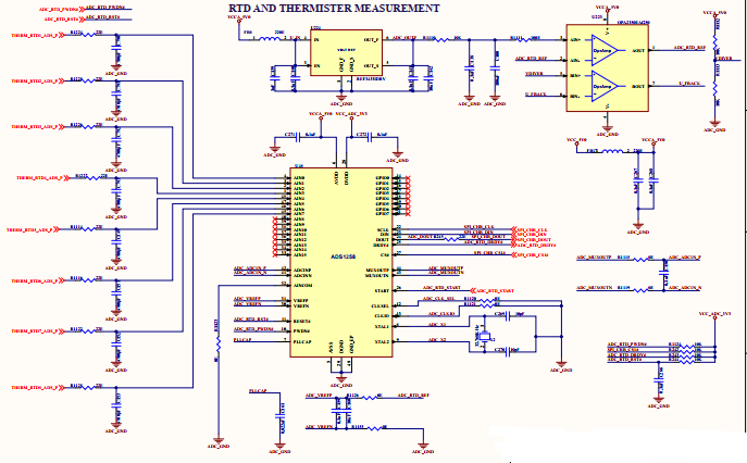
      Anybody Please Review our schematics and share your valuable feedback.

I have few  Questions.

1.How to terminate unused ADC channels and GPIO Lines, currently we are using only 8 ADC Channels.

2.external crystal has 70K series Resistance ,it is ok or we need to change the Different crystal.

3.AVSS and DGND we are using same GND.it is correct or we need to maintain separate GNDs. 

  • Hi Mahesha,

    I'd be glad to review your schematic and answer your questions...

    1. Unused inputs can either be tied to some voltage potential (between AVDD and  AVSS) or left floating.
      1. Floating inputs tend to have the lowest leakage current, but are often discouraged for EMI reasons.
      2. When tying unused input pins to a fixed potential, do not connect to a voltage potential that is > AVDD or < AVSS. Connecting to GND is typically the easiest implementation, but this does tend to have slightly higher leakages currents (typically on the order of nA) than tying to higher voltage potentials.

    2. The ADS1258 has a very low power crystal driver that has seemed to struggle with driver certain 32 kHz crystals. Typically, the higher ESR, the more power it takes to drive the crystal, so I generally recommend using a crystal oscillator (integrated crystal + crystal driver) whenever possible to avoid issues with crystal start-up. If you need to use a crystal, then try to find one with a lower ESR. I generally recommend 50kOhms or less.
       
    3. Excellent! I recommend connecting AVSS and DGND to the same ground plane (see https://e2e.ti.com/support/data-converters/f/73/p/755516/2790926 for additional details).

    Regarding the schematic, it was hard for me to make out some of the details in the compressed image (E2E may be to blame for this), so please bear with me, but but here are my suggestions:

    • Make sure to use buffered reference source such as the REF5xxx or REF6xxx devices. I wouldn't recommend using a REF3xxx series reference without an external buffer.

    • When routing the REFN signal, treat it as a differential signal and route a trace back to the ground pin of the reference source IC. Avoid connecting REFN to the ground plane (as it may pickup ground noise).

    • Avoid inductors on the supply rails. Precision ADCs don't like to have their supply currents choked, and also inductors can form LC resonators with nearby supply capacitors.

    If you have a high-resolution image or PDF of the schematic that you'd like me to take a closer look at. Please send it to pa_deltasigma_apps@ti.com.

  • Hi Mahesha,

    Thanks for sharing a PDF schematic with me!

    Is there any reason why you're not measuring the voltage across each of the RTDs deferentially and using a reference resistor (to make the measurement ratiometric), similar to the following configuration...?

    Figure 17 from SBAA275–Multiple Paralleled Four-Wire RTDs Measurement Circuit

    ...As long as each of the RTD have a similar nominal resistance, then you can probably share a single current source, reference resistor, and an external amplifier, for each of the RTDs. FYI: This image was taken from A Basic Guide to RTD Measurements.

    My additional suggestions would be to:

    1. Try to make the RTD measurement ratiometric (i.e. the input voltage an reference voltage change proportionally to the excitation current, which makes the measurement more immune to changes in the excitation current). If you follow the above scheme, you'll need to a a current source and MUX, but can remove the REF3433 and buffer.

    2. Add a differential amplifier between the ADS1258 MUXOUT and ADCIN pins. This will help to increase the signal amplitude as well as driver the delta-sigma modulator inputs.

    3. I would consider removing the ferrite bead on the 5V analog supply. In general, I think ferrite beads are good for removing noise on external connections that are connected to long wires. However, for on-board supply filtering I recommend using multiple decoupling capacitors of different sizes (0.1uF and 1 uF, for example). Multiple capacitors provide a "charge bucket" to the IC and keep the supply voltage stable during transient currents. Inductive components on the supply will tend to cause voltage spikes during current transients, and in some cases the choked current to the IC may degrade the performance of the device.