This thread has been locked.

If you have a related question, please click the "Ask a related question" button in the top right corner. The newly created question will be automatically linked to this question.

AFE0064: Abnormal data collection

Part Number: AFE0064

Dear All,

Thank you very much for your help!

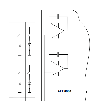
Technical problem of AFE0064:

1、Whether the following measured timing waveforms are used improperly;

2、Whether the differential signal output mode needs to be modified to 0;

3、Output whether the actual waveform is normal;

Problem Description:

1、The input signal is left floating, the detector is not connected, and the input reset switch is always off.

2、Afe0064 power supply 3.3v, reference voltage input 2.25v and 0.85v, output voltage 1.68v are normal;

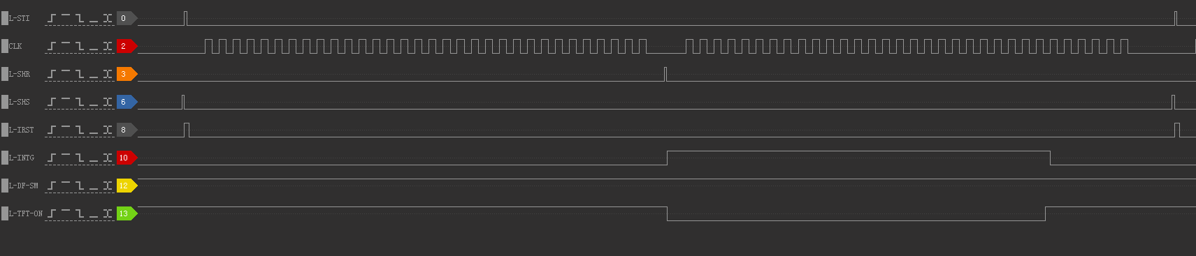
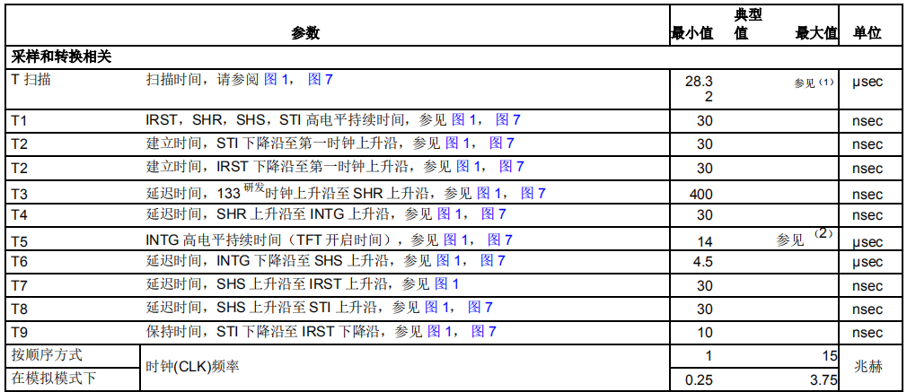
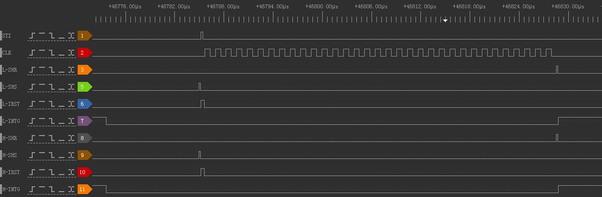
3、The control waveform timing is required, as shown in the following figure:


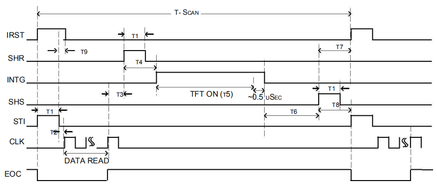
The timing waveform requirements are as follows:


4、The measured information is as follows:

Measured control waveform timing: T1 is 200ns, T2 is 250ns, T3 is 400ns, T4 is 250ns, T5 is greater than 14us, T6 is 11.3us, T7 is 250ns, T8 is 250ns, T9 is 200ns, all meet the timing waveform requirements;

 At present, the differential signal output port working mode INTUPz=1;


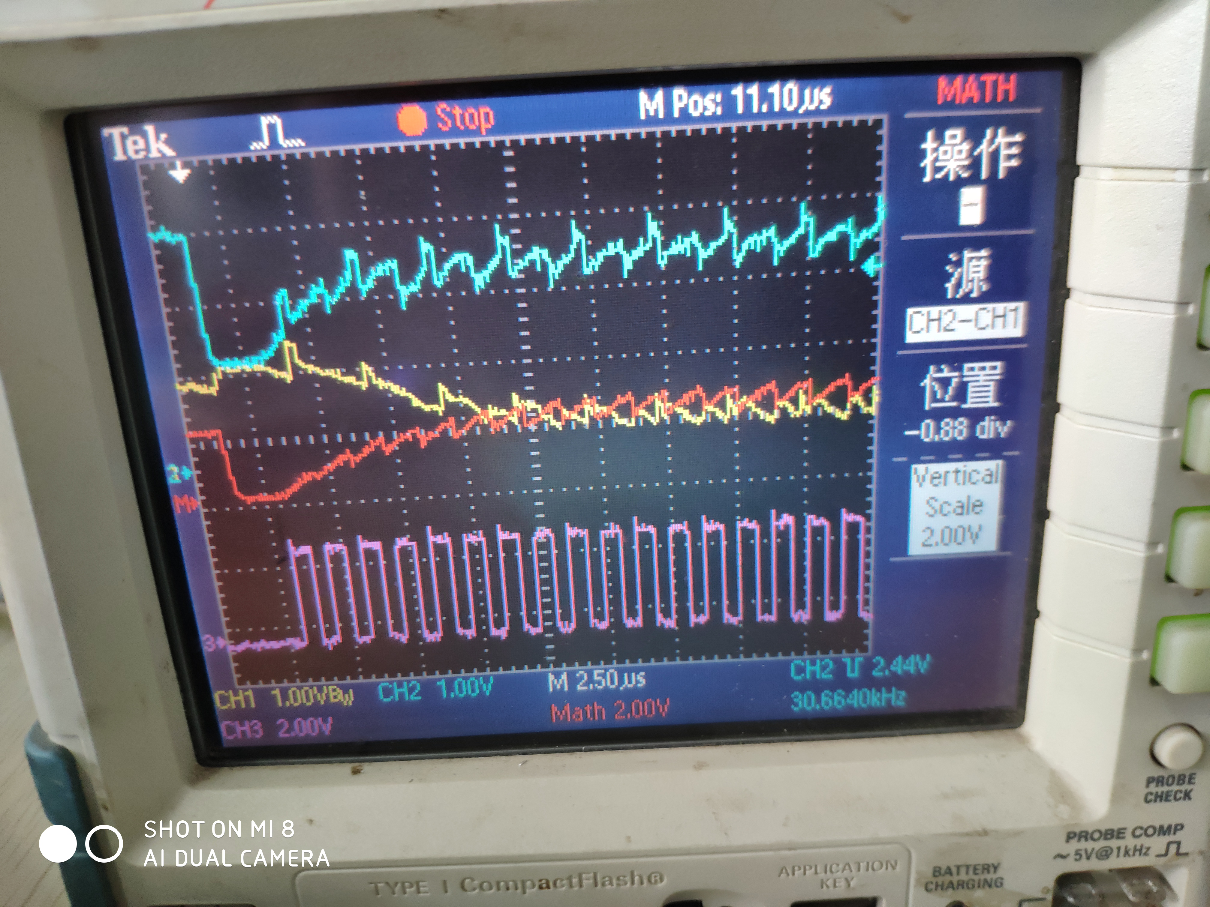
Measured waveform below:


The blue waveform is voutm, the yellow waveform is voutp, and the red is voutm-voutp.

Best Regards!

Lynn

  • Dear Lynn,

    In the control waveforms you have shown, the IRST is AFTER SHS. Also, the SHS signal is before SHR. However, the datasheet shows IRST must be before SHR followed by SHS.

    Can you please update the waveform duration and relative positions are as per the datasheet recommendation? After that, we can discuss the AFE0064's response to input signal.

  • Hi Lynn,

    We would like to take the conversation offline to discuss more details about your application.

    Please let us know if it is ok to send you an email to your email address registered at TI.com.

  • Hi Praveen,

    OK, I am  glad to communicate with you directly. Thank you!

    E-mail:sunchuanbao@zexin.net

  • Dear Shriram,

    Thanks for your reply.According to your instructions, we have finished the test again. Please help us to solve the new questions as follows. Looking forward to recieving from you.

    Technical problems:

    1.Please help confirm whether the connection of detector to AFE0064 input is correct.Shown in Figure 1;

    2.Please help confirm whether the control of AFE0064 timing waveform meets the control requirements.Shown in Figure 2;

    3.Please help confirm whether the output signal of AFE0064 chip is normal. Shown in Figure 3;

    First,our connection between detector and AFE0064 is the silicon photodiode array.The connection method is shown in Figure 

    Fig.1

    The connection is a common cathode connection, the cathode end is connected to AFE0064 VREF (1.65v), and the anode end of the detector is connected to the AFE0064 input through a switch. Please ask a TI technical engineer to help us confirm whether this connection is feasible.

    Second,the control AFE0064 timing waveform is shown in Figure 2


    Fig.2 (The frist SHS is the signal of the previous period)


    Measured control waveform timingT1 is 200nsT2 is 250ns,T3 is 400ns,T4 is 250ns,T5 is required to more than 14us,T6 is 11.3us,T7 is 250ns,T8 is 250ns,T9 is 200ns.All of the above meet the timing waveform requirements

    Third, is the AFE0064 output differential signal terminal.

    The current differential signal output mode is INTUPz=1;

    Under the daylight detection state, the measured waveform is shown in Figure 3.


    Fig.3

    We can see:the blue waveform is VOUTM, the yellow waveform is VOUTP, the red is VOUTM-VOUTP, and the purple is the CLK clock signal.

    What’s more,in the first 5 CLK cycles, the differential output signal is distorted, and the next 59 signals output amplitude is around 2V.

  • Hi Lynn,

    I am closing this post since the discussion has been taken offline.