This thread has been locked.

If you have a related question, please click the "Ask a related question" button in the top right corner. The newly created question will be automatically linked to this question.

ADS8598H: Common Mode Rejection

Part Number: ADS8598H

Hello

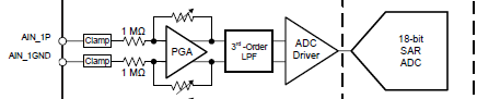
How much CommonMode Rejection can I expect from the ADS8598H? Our setup is as shown in the following picture. The datasheet only mentions that the source impedance of the positive and negative path allows for better common mode rejection but does not give any quantitive information (Rejection vs frequency).

If you have any measurement data, that would be great, otherwise a rough estimate would also be appreciated.

Best regards

Haje

  • Hello Haje,

    ADS8598H is a single-ended input ADC and does not support differential input signal, this is why there is no common-mode rejection specification and information. Also, the Electrical Characteristics table in the data sheet has showed the input restriction, please see below:

    Thanks&regards,

    Dale

  • Hello Dale

    Thank you for your reply.

    I'm aware of the +-0.3V limitation on the AIN_nGND pin. I interpreted this as the the maximum amplitude of common-mode signal (between AGND and AN_1GND) that the ADS8598H can handle.

    I also understand that the input is not for true differential signals but to me it looked like single-ended with "GroundSense" (not sure what the correct term is).

    The signal chain (picture below) looks differential to me and I would have expected some common-mode rejection by the differential amplifier.

    If that is not the case, what is the benefit of having a ground pin per channel?

    Best regards

    Haje

  • Hi Haje,

    The analog front-end (AFE) structure on the device is a part of internal design topology. I will let you know if we have similar device to support differential input in the future, however, this ADS8598H ADC only support single-end input signal, a matching resistor on the AIN_xGND pin as a balanced input RC filter can be used to cancel additional offset error contributed by the external resistance, but the potential voltage on this pin should be limited to +/-0.3V range. To convert a signal with higher common-mode voltage, a instrumentation amplifier or difference amplifier can be used before the ADC, please see an circuit design as below:

    High common-mode differential input voltage to ±10-V ADC input circuit

    Thanks&regards,

    Dale

  • Hi Dale

    I'm interested in the rejection of small voltages, within the +/-0.3V range.

    As an example:

    0.1V 50Hz Vcm (as in my first picture) between AGND and AIN_1GND

    Will there be really no rejection and I will see the full 0.1V on the digitized signal?

    Best regards

    Haje

  • HI Haje,

    Unfortunately we do not have this kind of data, AIN_xGND pin is assumed to be connected to the ground directly.

    Thanks&regards,

    Dale