This thread has been locked.

If you have a related question, please click the "Ask a related question" button in the top right corner. The newly created question will be automatically linked to this question.

ADS8568: Need Simultaneous 32 Sensor real time data using ADS8568 - All reading must be simultaneous

Part Number: ADS8568


Hi TI Team,

I am working on the redesign of the existing Sensor based system and this is the first phase for me and our company.

Specifications/system configuration in existing hardware is as below:

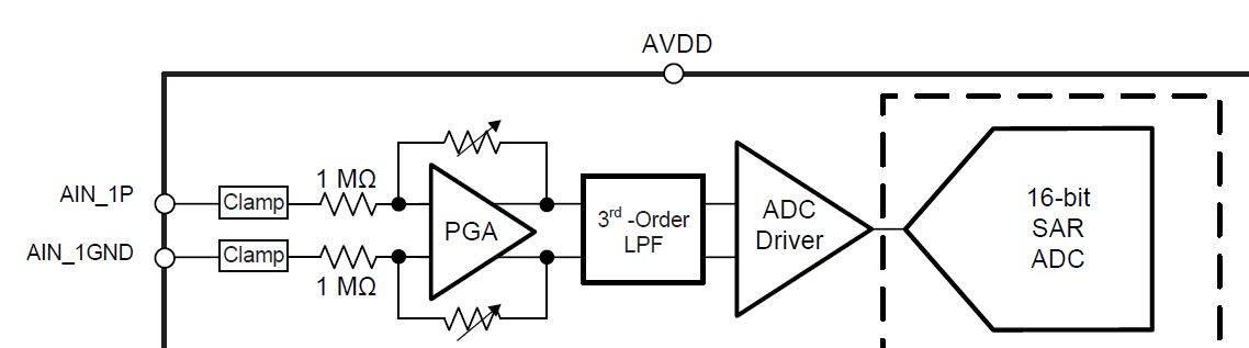
- It has four ADS8568 ADCs to take the data simultaneously of all 32 channels (4x8 channels) and must receive data at same time for all 32 channels. (Currently receiving data simultaneously within the 8 Channel ADC but could not get sync with all external ADC Channels) (Image as per below) )

- Using four different SPI (each ADC have a separate SPI) connected with Processor(i.MX6)

- Four CONVST signal(each ADC have a single CONVST connected with processor and within ADC all the CONVST_A,B,C,D is shorted)

- input support 0 to +/-45V and using resister divider with AFE to limit to +/- 12V

- Set the reference voltage internal to 3V and +/-4VREF to support +/-12V input

- Using SW (Software) method support in ADS8568

To redesign the existing system, I need to debug the existing system to achieve the synchronization between all the 32 channel and must receive data simultaneously especially with external all four ADCs.

So, I need TI expert help to achieve this goal and to successfully redesign the new hardware,

1. Will I need to common all four CONVST signals connected with the four ADCs?

2. Is that HW or SW configuration will give the better results or low latency?

3. Daisy chain will help here or will receive more latency than seperate SPI?

4. Is that I need to give External common Clock at XCLK to all the ADCs?(Existing system is using internal clock only)

5. Is that I need External VREF which will be common to all four ADCs? Is that effect the synchronization?

6. Will I need to Monitor/use BUSY/INT signal connect with processor to take readings/conversation in sync for the next sequence of data?

7. Will it Parallel mode(Digital IOs) is better or Serial mode(SPI) to get the data simultaneous using processor?

8. Is that Processor based design will work or need to select FPGA or CPLD for the new design based on your expertise for the ADC data sync?

Let me know if you need more details regarding existing system.

Thank you,

Nilav Choksi


  • Hello Nilav,

    Thank you for your post.

    Synchronization of all four ADS8568 devices (and all 32 channels) is certainly achievable. 

    1. Yes, you do need to use a common CONVST signal. Assuming that you want all 32 channels to operate at the same data rate, you can share one common CONVST signal to all 4 devices and their respective CONVST_A, CONVST_B, CONVST_C, and CONVST_D pins can all be shorted together.
    2. The HW or SW configuration mode has no effect on the device latency. This mode selection simply configures the device using hardware mode pins or software register settings.
    3. Daisy-chaining devices does not affect the latency, but it will simplify the number of connections required between the ADCs and your host controller. You may use either the serial interface or the parallel interface in a daisy-chain configuration.
    4. Using the internal or external conversion clock will work equally well.
    5. The reference voltage source will not affect the latency or the device synchronization. The only effect that using different reference voltages will have is a gain error. You may use the internal 3-V reference on each ADS8568 device and then calibrate the gain and offset error for each ADC separately, if needed.
    6. Yes, you must monitor the BUSY signal in order to know when the conversion period is complete. After BUSY transitions low, the conversions are completed for all 8 ADCs inside the device. Then, you may clock out the data using whichever interface mode you choose.
    7. Both interface modes will allow you to achieve simultaneous sampling among multiple devices. However, the parallel interface can achieve faster overall throughput, which enables you to achieve the maximum output data rate.
    8. The processor selection only depends on the required connections for the ADC interface and does not depend on the synchronization. In other words, you only need to verify that your processor can provide the necessary inputs/outputs, such as CONVST, SDOx, /FS, BUSY, etc.

    The main point to remember here is that you have two separate design decisions. First is the synchronization of all 32 channels. This is achieved simply by sharing one common CONVST signal to all four CONVST_X pins on all four ADS8568 devices. Once you see BUSY transition from high to low, the conversion process is completed and you can read the data.

    Second, after conversions are completed, the rest of the device communication is only for reading the data out (simultaneous sampling has already been achieved at this point). You can daisy-chain all four ADS8568 devices and choose whichever interface mode you prefer (serial or parallel):

    • In serial interface mode, you will read data from the four SDO_X pins in the last device in the chain. See Figure 41 in the data sheet.
    • In parallel interface mode, 16-bit data from each channel (A0, A1, B0, etc.) is read on pins DB[15:0]. All four ADS8568 devices will require separate /CS signals (i.e. /CS1, /CS2, etc.) in order for DB[15:0] to be shared. Enable /CS1 for the first device and use /RD to progress from A0, to A1..., etc. (/RD can be common to all four ADS8568 devices). Then disable /CS1 and proceed to enable /CS2 and so on. After all data is read, you can begin a new conversion cycle.

    Best regards,

  • Hi Ryan,

    Thank you for your quick reply and sorry for the delayed response.

    This is definitely helping us for the current system debug and new deign development.

    Based on your answers, I have below points/questions,

    1. As per Answer 3, Will it receive same sync result between four different ADCs(conversion and reading) using four separate SPI interface or single SPI with different four CS pins or Daisy chain SPI method as per Figure 41 in datasheet?(We want to achieve data-rate upto 40Ksps only.)

    2. Is there any external mechanism required to sync all internal reference clocks to be sync(if we use internal clock) or power supply sync of ADC will work for this case?

    3. Is the External reference clock more suitable to sync all ADCs to get the exact sync?(to remove more ppm difference)

    4. How can I calibrate the gain and offset error for each ADC separately? Is there any recommendation part of Op-amp?

    5. To achieve the external ADC synchronization including conversion and reading data, Is that possible to read the all 32 channel data simultaneously with processor? (currently using processor which has all the connections and configuration with ADCs are also same as per your recommendation). It would be good if you can share practical use case with practical if any.

    Let me know if you need more details.

    Thank you Regards,

    Nilav Choksi.

  • Hello Nilav,

    1. The synchronization timing is controlled by CONVST only. This signal must be shared with all ADS8568 devices to achieve true simultaneous sampling. Once the CONVST signal transitions from low to high, the device latches the voltage on the sample-and-hold capacitor circuit. Sampling is complete at this point. From this moment forward, all channels have sampled the input voltage at exactly the same time and it does not matter how long it takes to convert and read the data. The conversion process begins based on the internal or external clock of each device. You only need to monitor the BUSY signal for each device to know when the conversion process completes (you could also use a NOR gate and when all BUSY signals go low, the output will be 1). Once the last device finishes converting, you may read the data using either a single SPI bus (with 4 separate /CS signals), a daisy-chain configuration, or 4 totally separate SPI buses. The important thing here is you must finish reading all of the data before issuing the next CONVST pulse in order to maintain the desired data rate.
    2. No, as per #1, it is not necessary to synchronize the internal clocks.
    3. No.
    4. The process for each channel is the same. You must provide at least two precision inputs to each channel and record the average output. This will allow you to draw a line of best fit and derive the offset and gain error coefficients for each channel.
    5. Even for just a single ADS8568 device, it is not possible to read all 8 channels simultaneously. The fastest data transfer is achieved using the parallel interface, which outputs a single 16-bit word for each channel, one channel at a time. So with 4 ADS8568 devices, assuming you have 4x 16 MISO pins on your MCU, you can read at most 4 channels at a time.

    Best regards,

  • Hello Ryan,

    Thank you for the in brief details and clear doubts,

    As per #5 response, Currently we are receiving all 8 channel data reading simultaneously but the pin point is, I also want to read all 32-channel data simultaneously.

    e.g. - If I apply Sine wave at input, it must receive same data at same time of all 32 channels.(conversion and reading both must be synchronized/simultaneous).

    As per #5 response, It results, I can't read all 32 channel data simultaneously and can not get the same response same time with processor, Is it correct? If yes, so can this achieve with FPGA by interface parallel interface?

    Note: Here, the data rate requirements is low upto 30KSps to 40KSps only.

  • Hello Nilav,

    Let me clarify what I meant in my response to #5. "Simultaneous sampling" only refers to capturing the analog input voltage on all 8 channels at precisely the same moment. This is guaranteed by sharing the same CONVST signal to all ADS8568 devices. An analogy we sometimes use would be "sampling the input voltage is like handing in your exam. The time is up and all answers are final."

    After the input voltage is captured, the conversion process takes place internally. This would be analogous to "grading the exams, one by one." It doesn't matter how long it takes to grade the exams - the answers are already handed in. Likewise, the duration of the ADC conversion time depends on the internal clock frequency, but the end result at the output will be the same. Once the conversion is complete, you can read the data using any of the following methods:

    1. 1 channel at a time (parallel interface, pins DB[15:0])
    2. 1 channel at a time (serial interface, SDO_A only)
    3. 2 channels at a time (serial interface, SDO_A and SDO_B)
    4. 4 channels at a time (serial interface, SDO_A, SDO_B, SDO_C, and SDO_D)

    Regardless of which method above you choose, you will be able to read the data from all 8 channels on each ADS8568 device. The exact moment that the conversion result is read does not change the value at the ADC output; therefore, reading 32 channels at once is not required to achieve simultaneous sampling.

    This same principle applies to using multiple ADS8568 devices. You may share the data lines (DB[n] or SDO_x pins) across multiple ADS8568 devices as long as you maintain separate /CS signals for each device. Or, you can daisy-chain the ADS8568 devices together and use interface method #4.

    What is the frequency of the interface clock that you plan to use in your application? I can verify which of the methods above will allow you to achieve up to 40 kSPS data rate.

    Best regards,

  • Hi Ryan,

    Thank you for giving the detailed understanding for the ADC conversion and reading operation,

    Currently, I am planning to use 10MHz and can use upto 30MHz SPI clock frequency, Is this sufficient to read all 32 channel data before next CONVST signal?  

    What is the timing between the two next CONVST signal for the ADCs?(Our sensors will read data continuously) Is timing sufficient to read all 32 channel data before next CONVST pulse?

  • Hello Ryan,

    I have calculated the theoretical timing for the CONVERSION and READING is as per below, so, is this correct method?

    Conversion time for 1 ADC = 30kspsx16x8=3.84microsecond is parallel/simultaneous for all ADC

    Reading time for 1 ADC(if SPI operate at 30MHz) = 33.33ns so total time for reading for 4 ADC = 4x33.33= 133.33nS + 3xscheduling delay between each ADC(~100ns) = max. 500ns time which is higher than 280ns(tacq) time.

    So, it means we need to maintain minimum 4.4us delay between two conversion pulse. Is this correct? Is timing sufficient to read all 32 channel data before next CONVST pulse?

    Waiting for your quick response.

    Thank you,

    Nilav Choksi

  • Hi Nilav,

    The time between consecutive CONVST rising edges sets the ADC sampling rate. For 30 kSPS, all 32 CONVST_x pins (which are shorted together), will see the same rising edge every 33.33 us (i.e. the sampling period). In other words, you have 33.33 us for the conversion time + reading data. Any unused or "extra" time is perfectly fine.

    The conversion time is fixed when using the internal conversion clock. A maximum tCONV spec is provided in the data sheet for the ADS8568 as 1.7 us. This time is useful for planning your interface, but in practice, your MCU will be monitoring the BUSY/INT pin to precisely detect when the internal conversions are completed. If all 8 channels are simultaneously sampled (i.e. all CONVST_x pins are tied together), you can use the interrupt function of the BUSY/INT pin, which will indicate when all ADCs are done converting.

    After the conversion time, you need to clock out the conversion data. Each channel has 16 bits of data. The time required to read all data is calculated as 16 bits x "channels per SDO" / SCLK frequency. For example, if you are using all 4 SDO pins (A, B, C, and D), you will be reading two channels of data on each SDO (i.e. CHA0 and CHA1 are read from SDO_A). So, 16 bits x 2 / 30 MHz = 1.067 us to read the data.

    In total, you need to read 16 bits x 32 channels = 512 bits of data. With SCLK = 30 MHz, you could read all channels on a single SDO up to ~58 kSPS (technically a little less to account for all timing specifications). Any combination of reading data in parallel will work for your application and perhaps allow you to slow down your SCLK frequency.

    Best regards, 

  • Hi Ryan,

    Thank you for clear all the doubts and based on the discussions we are also debugging our existing system.

    During the comparison of different simultaneous ADC, I came across ADS8588 which also looks same as ADS8568 including AFE portion.

    For New design, I am planning to use ADS8588 so is it also works to get the data simultanously read all 32 channels?

    Note: Our input is PZT sensor (range +/-45V)

    Regards & Thank you,

    Nilav Choksi

  • Hi Nilav,

    I'm glad this helped to clarify things for you.

    The ADS8588 is also an 8-channel, simultaneous-sampling device. However, the input impedance of the ADS8588 is much larger (about 1 M). There is a PGA stage at the input of each channel, which can be configured to accept +/- 10 V or +/- 5 V input voltages. You will need to attenuate the PZT sensor output before connecting to the ADS8588 input. Also, the inputs must be single-ended with respect to GND and connected to AIN_xP.

    ADS8588 Block Diagram:


    The ADS8588 has two CONVST pins which can be shorted together for simultaneous sampling. This device also offers parallel interface options similar to the ADS8568. You should have no trouble achieving 32 channels at 30 kSPS.

    Best regards,

  • Hi Ryan,

    Thank you for the ADS8588 related answers but still I am stick to this part as the AFE is inside the ADC and which reduce my cost and extra circuitry and work with piezoelectric transducer(PZT sensor).

    Can I use Daisy chain method with single SDO instead of 4 SDO_A,B,C and D to achieve 30KSps datarate? (same as per Normal serial configuration: SEL_B and SEL_C,D=0 mentioned in Figure 39).

    Also, I am concluding this thread,

    1. Need to common all CONVSTA,B,C and D signals of all 4 ADCs. (total current will be 800nA which can drive by the Processor)

    2. Need to monitor BUSY signals of all 4 ADCs with NOR circuit.

    3. I will use Serial SPI interface with 4 chip select and single SDO_A instead of all four SDO_A,B,C or D to achieve 30KSps(as per calculation max. is 58kSps)

    Or else suggest (Need to use four SDO or need to use Daisy chain with four SDO or parallel to achieve 30Ksps rate or more.(Processor also have scheduling delays for the operations)

    4. Will add external voltage reference circuit as an option(first use internal reference)

    5. Will add external clock reference circuit as an option,(first use internal reference)

    Also, In the existing system, we have common all four CONVST signals of all 4 ADCs and we are running the application, here we are receiving nearly 120uS of High pulse(CONVST high pulse on oscilloscope) so is this define the sampling rate or I need to check the timing between two rising edge of CONVST signal(which is always more higher than the CONVST(High) pulse)? If it so, I am not achieving the sampling rate and getting upto 8Ksps(1/120uS) 

    Here am I missing something? or please share yout thought/suggestions.

    Thank you,

    Nilav Choksi

  • Hi Nilav,

    Yes - I mentioned in my previous post that 30 MHz SCLK would allow you to read all channels on a single SDO if the desired data rate is only 30 kSPS.

    1. Yes
    2. NOR circuit is not required, just an idea if the individual BUSY signals are not synchronized. In your application, all CONVST are shared for daisy-chain configuration. If bit C.27 and C.26 = 0, you should only have to monitor one BUSY signal per figure 41.
    3. ok
    4. ok
    5. ok
    6. CONVST rising edge defines the data rate.

    Best regards,

  • Hi Ryan,

    Thank you for all the answers and points to solve the queries.

    Last questions, Have you seen any practical applications/existing design where the multiple channels(32 or more channels with multiple ADCs) achieved simultaneous operation with min. 30KSps using Processor/Cotroller? because in our existing system once we common all four ADC CONVST signals, we are receiving 120uS of High pulse(CONVST High period).

    If yes, can you please share the application details which gives up better confidence for the new design.

  • Hi Nilav,

    If your controller is unable to maintain the CONVST_x period required for 30 kSPS (33.33 us), then you will likely need to adjust how the firmware is structured. I believe your processor should be more than capable of acquiring all the data, but perhaps some other routines are introducing too much delay. One suggestion might be to try acquiring the data in parallel per one of the options I previously described. Acquiring the data faster may allow your processor more time for other computations before the next sample is acquired. I'm not a DSP expert, so I cannot help you further with software development.

    Best regards, 

  • Hi Ryan,

    Currently, our firmware team is using the standard linux system without any other application running. Still we are achieve upto 8KSps of sampling rate. However, our team is working on it and thank you for your all support.

    Can you please share me the driver for ADS8568 and ADS8588 as we are currently working with ADS8568 and need to validate the driver and as we are switching to ADS8588.

    Best Regards and Thank you,

    Nilav Choksi

  • Hi Nilav,

    I'm sorry, but we do not have Linux drivers to provide for these devices.

    Best regards,