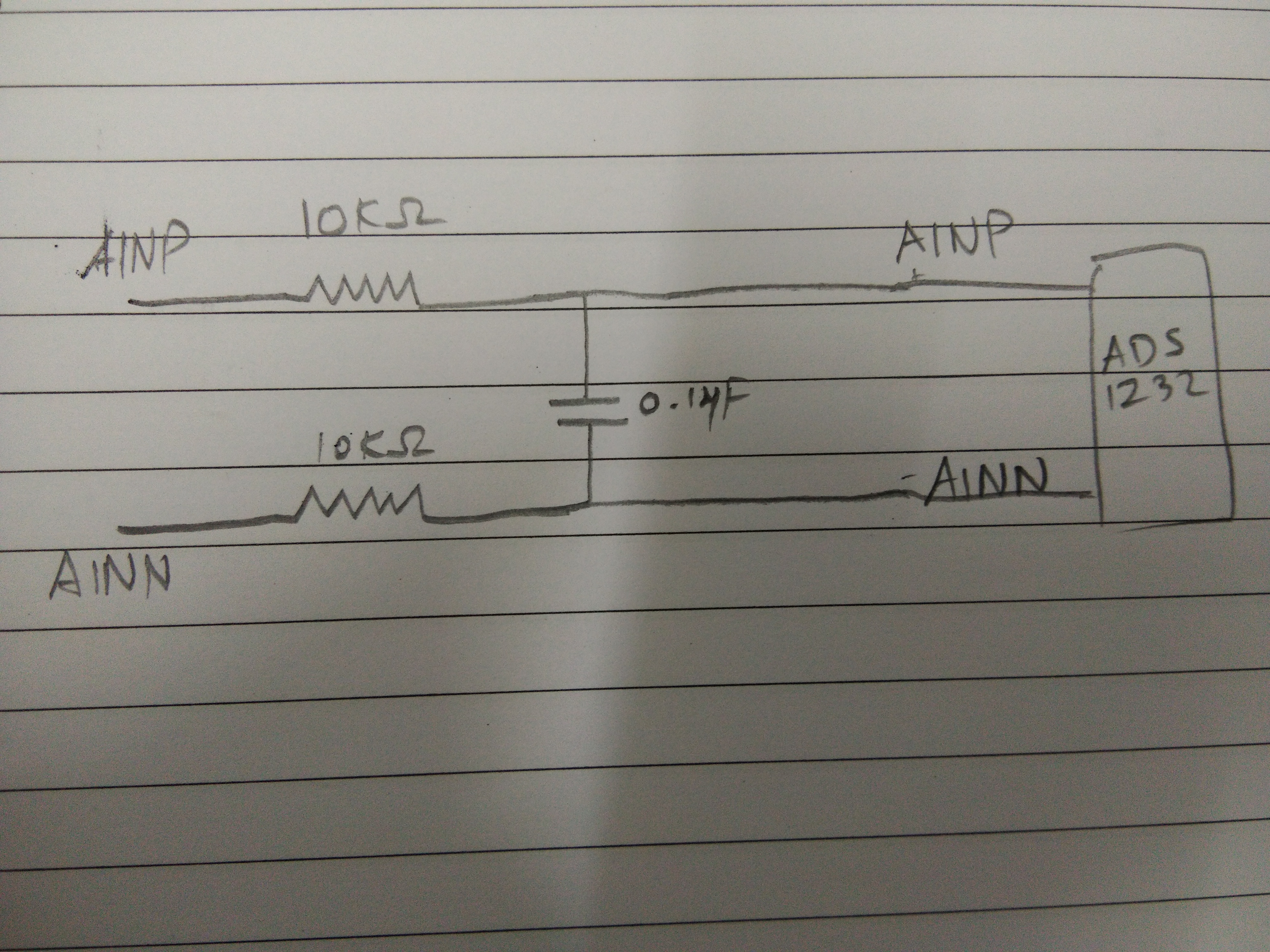
This thread has been locked.

If you have a related question, please click the "Ask a related question" button in the top right corner. The newly created question will be automatically linked to this question.

ADS1232: ads1232

Part Number: ADS1232

Hi Bob,

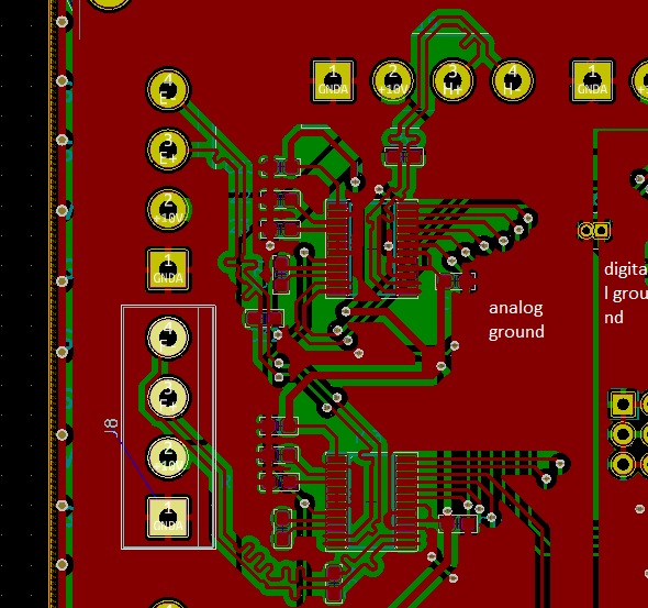
I am using a filter circuit for the input which I have attached. But I see wrong values in the input pins. Is there any problem with the filter circuit?. Also I have attached the screenshot of digital ground and analog ground that I have shorted. If it is a problem then should I connect the digital and analog grounds through an inductor?

  • Hi Gobinath,

    As I recall you are using an excitation of 10V which places the common-mode at 5V.  This puts you in a situation where you can only use a gain of 1 or 2, which bypasses the high impedance PGA and uses a much lower impedance switched cap input.  So a 10k input resistor may be too large for this configuration.

    However, we still haven't determined what the real problem is as I don't have enough information.  Most likely what you are seeing is error due to noise with respect to the input path and the reference.  As the measurement is not ratiometric, the reference noise and stability (drift) will be directly proportional to the measurement.  The input path itself may have a lot of noise from EMI/RFI.  To help determine what the true nature of the issue is we would need to know the precise input voltage with a minimum of 256 (up to 1024) consecutive and contiguous (where every result is captured for a particular input with no gaps) so that we can plot them. 

    The ADS1232 was designed to achieve the highest performance by using 5V excitation with the reference using the same voltage source as the excitation.  This allows the common-mode to be at 2.5V where a gain of 128 can be used.  Input-referred noise actually lowers with PGA gain.  Your system is not taking full advantage of the ADC design to get the highest level of performance.  What you are able to achieve is only a fraction of the converter range and perhaps that is good enough for your application.  However you will experience drift, and as I have stated to you before, you may run into issues with the output of the bridge exceeding the input range of the ADC causing a linearity error.

    Also, you should try shorting the inputs together at the ADC inputs to see if you can achieve the level of performance shown in the noise tables shown on page 5 of the ADS1232 datasheet.

    There could be substantial noise pickup due to the PCB layout.  The best practice is to use a solid ground plane under the analog input traces and also keep the low-level analog input traces out of the digital domain.  With as many ADCs and inputs as you are using this becomes very difficult.  Achieving high performance requires a specialized layout.  One of my colleagues has put together an FAQ regarding PCB layout:

    https://e2e.ti.com/support/data-converters/f/73/p/755516/2790926?tisearch=e2e-quicksearch&keymatch=FAQ#2790926

    Absolutely do not add inductance (or even a ferrite bead) between the analog and digital grounds.  It would be much better to separate the analog and digital traces so that they do not cross each other and to use a single ground plane.  Adding inductance can cause the device to exceed the Absolute Maximum Rating of +/-300mV between analog and digital grounds.  Any noise or transient with a fast rise time can exceed this limit.

    I would suggest looking at the ADS1232REF user's guide for an example of a layout that uses a 2-layer board with a single ground plane where no analog and digital traces cross paths.

    Best regards,

    Bob B

  • Hi bob ,

          I am applying 10V common mode voltage. But It was working fine with 1k series resistor for a certain period of time.After that same specification without 1k series resistor is  working, But with deviations in the output around [ 0.1mV , 0.2mV ],is there any suggestion for improving the accuracy of  output with respect to the input.

                         thank you,

  • Hi Gobinath,

    I'm not totally sure I understand your last post.  You cannot have 10V common-mode as that is outside of the input range of the ADS1232.  I think you are saying that you are applying 10V excitation which would result in 5V common-mode for a balanced bridge (1/2 of the excitation).  Is that correct?

    We started the thread with 10k series resistors and you saw an error.  Most likely this error is due to the lower input impedance of the bypassed PGA.  Then I think in this last post you are saying that 1k was working.  Then you removed the 1k resistors and now you are seeing a difference in the output of 100 to 200uV.  Another question I have is why did you stop using 1k if it was working?

    Next question, what is your actual input voltage?  And what is the code value being returned (with no calculation)?  What value are you using as the reference voltage in your calculation?  Have you measured the reference voltage?  As you are not making a ratiometric measurement, you must use the precise value for the reference in your calculation (or you must calibrate to the reference). A 5V reference calculation will return a much different result if the true voltage is 4.95V or 5.05V.

    The last thing I wish to note is you are not using the ADC in the manner intended.  The ADS1232 was designed to use the same excitation voltage as the reference voltage with a common-mode voltage within the input range of the PGA so that the measurement is ratiometric.  The PGA allows for a higher impedance input and allows measurement with gain for small input signals.  This is how you get the best performance from the device with the most precision.  It is difficult for me to advise you on getting a high level of performance as the potential error is quite high using the system you have developed.  Functionally it will work assuming you have not violated any of the input restrictions.  But the measurement will never be as accurate or precise as the recommended system. 

    Best regards,

    Bob B

  • Exact input is 1mV differential signal while looping the input to both of the channels i got output count value CH0 = 3202 (decimal) CH1 = 3464(decimal). while calculating the voltage using reference voltage +5V. I am getting this vaues like CH0 = 0.9mV, CH1 = 1.032mV. Inspite looping the the channel with 1 mV. I am getting difference in output voltage. this variation comes while connecting my loadcell with +5V and +10V also .


     CALCULATION EXAMPLE i am doing :  
    voltage  =[reference voltage / 2^(24-1)] / count .
    voltage  =[ +5V / 16777215 ] * 3202
    will you please recommend any RC and LC fillter or calculating formulas 
                thank you,
  • Hi Gobinath,

    Please re-read my last two posts.  I need many data points to ascertain the level of noise. One point does not tell me that.  Also, 5V is not your reference.  You need to directly measure it.  It might be 5.02V but this will calculate out differently than an assumed value.  Also, as the measurement is not ratiometric, this voltage can change due to drift and so can your result.

    To check your offset between channels you first need to issue the self-offset calibration after the reference supply has settled to its nominal voltage.  You then need to apply an external short (by shorting the inputs together).  At a gain of 1 you can short the inputs to analog ground.  When using higher gain (64 or 128) you would need to create a voltage divider using equal value resistors between AVDD and AGND.    The junction of the resistors would then be connected to the shorted input so that the input voltage is in the correct common-mode input range.

    You then need to compare the result between channels and also compare to the noise tables in the datasheet.  To determine the noise, you cannot just take one sample.  You should take a minimum of 256 and better yet 1024 samples as that is what is used for the noise-tables.  These samples must be continuous and contiguous (meaning that there are no samples missed or skipped).  Once we have some of this data we can move forward with recommendations.

    Best regards,

    Bob B

  • Hi Gobinath,

    Were you able to collect any data for me to analyze?  I think that a lot of the deviation you are seeing is due to noise.  This could be power line-cycle noise and/or issues with noise from digital signals getting into the analog due to non-optimal PCB layout.

    Best regards,

    Bob B