Hi everyone,
I am designing a ADC/DAC pcb which includes two ADS42JB46, and one DAC38J84. I have few questions.
1- DAC's RX lines doesn't have to be length matched I guess? (Of course two differential lines should be length matched)
2- Likewise ADC's TX lines doesn't have to be length matched, am I correct?
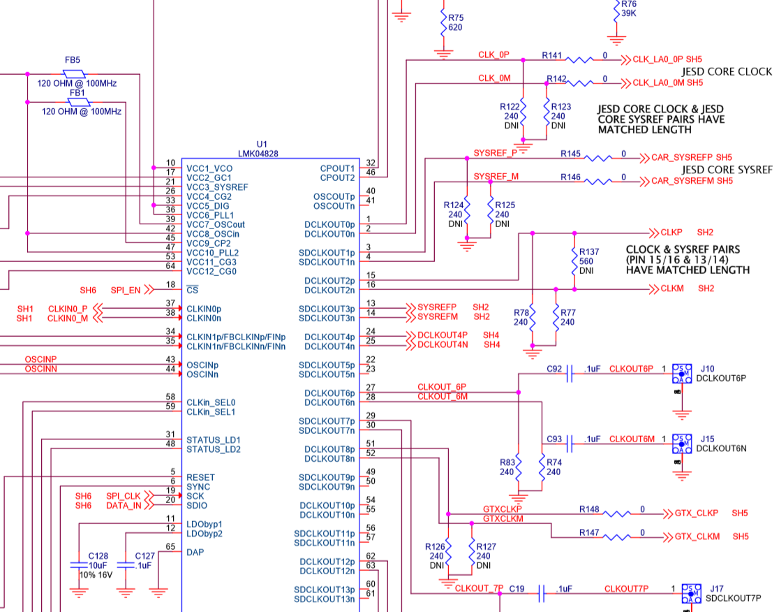
3- ADC's SYSREF and CLKIN should be length matched right? But I don't know if all ADC1's ADC2's and DAC's SYSREF and CLKIN should be length matched?
4- I don't know if SYNC lines should be length matched to other differential line?
Thanks in advance.
Canberk