This thread has been locked.

If you have a related question, please click the "Ask a related question" button in the top right corner. The newly created question will be automatically linked to this question.

ADS1262: SPI read problem

Part Number: ADS1262
Other Parts Discussed in Thread: ADS1256, ADS124S08

Hello. I use ads1262 to measure +-2 volt in bipolar mode, CS and START(for start conversion use START1 command) connected always GND, DRDY to MCU interrput. ADC clock modes external crystal 7.3728 MHz. SPI isolation adum1402A.Configuration SPI - clock 750 Kb/s (PCLK2 24 MHz, SPI prescaler 32), CPOL 0 CPHA 1, MSB first. MCU stm32f100c8t. I have problem to read or write configuration register. Read conversion result have not tried it yet. Almost no response to commands or wrong data, sometimes the data is correct. How to solve this?

SPI signal clean, antiring resistor 22 ohm, pcb tracke short. 

  • Hi Boris,

    Are you using a 24 MHz SCLK for the SPI communication?
    The ADS1262 can take an SCLK of up to 8 MHz. Try a slower SCLK frequency and see if that helps resolve things.

  • 24 MHz peripheral clocking. SPI has a frequency of 750 kHz after prescaler. I tried to set the frequency from 93 kHz to 1.5 MHz, without result.

  • Hi Boris,

    OK, that should be fine.

    When you looked at the SPI signals, did they appear clean on both sides of the isolator?

    Another thing to check is to make sure that you aren't communicating with the ADS1262 too soon after power-up. There is a time period after powering up the device where the device is internally held in a reset state. Typically, I wait even longer than this period, and use the first /DRDY falling edge as an indication that the device is actively communication and ready for communication. Do you see a consistent /DRDY period being outputted from the device? 

  • The signal looked of ads1262 pin. /DRDY is always high since /START is always connected to gnd. I wanted to start the conversion with the command START1. The documentation says that when power is applied, the start time is 2^16 ~9 ms. Waiting even at 1 minute for no result.

  • Hi Boris,

    OK, do you see /DRDY go low after issuing a START1 command?
    If not, then either the command is not getting interpreted correctly, the nPWDN/nRESET pin is low and the device is being held in a power-down mode, or perhaps the ADS1262 does not have a valid master clock signal.

    Have you checked that state of the nRESET/nPWDN pin?

    Also, how is the ADS1262 being clock; are you using an external clock/oscillator, or the internal oscillator?

  • The START1 command does not always succeed, like any other. But if passed, then pulses appear on the pin /DRDY. When trying to read configuration, invalid data.

    nRESET/nPWDN is connected through 10k to DVDD (3.3 volts), not low.

    Clock ADS1262 external crystal 7.3728 MHz. Pure sine wave signal.

  • Hi Boris,

    It sounds like the the device is clocked and active, so at the moment my guess is there must be some sort of a timing issue on the SPI communication.

    Would you be able to capture and share an oscilloscope screenshot of the SPI signals (on the ADC side), during one of these ignored commands, or command(s) that result in an invalid response from the ADC? I can review the image for you to see if I can spot any potential timing issues.

  • I found a problem. The power of the ADC and the microcontroller is galvanically isolated. The problem occurs if you first connect the power to the ADC, and then to the microcontroller. The ADC freezes, then when you try to send a command or data, it randomly turns off. When you try to check the level (after your request) on nRESET / nPWDN, the ADC starts immediately, because of this, it always seemed to me that it was turned on. After that, if do not turn off or turn on the microcontroller, then the ADC works fine. Since the digital isolator is 2/2 configured, the problem is with SCLK or MOSI. High level or noise for a short time on pins 11 and 12 can lead to a freeze or malfunction of the ADC?

  • Hi Boris,

    Excellent, I'm glad to hear you were able to identify the cause of the problem!

    To me it sounds like the ADC may have seen some extra SCLK edges while the MCU was not driving this signal. In this case, the the ADC may have been a few SCLKs ahead of the MCU, resulting the MCU commands being mis-interpreted.

    One thing you could do after powering the MCU, is to configure the SCLK pin as a GPIO pin and transition it from a low to a high state, and hold it high for about 10 ms. After the first SCLK rising edge, if the ADS1262 does not see another SCLK for within 65536 fCLK periods, then the serial interface is reset and can be re-synchronized to the MCU's serial clock. Refer to section 9.4.4.4 (pg. 66) of the ADS1262 datasheet for additional details on this behavior.

  • One more thought.... Maybe by ensuring that the digital isolator is not enabled until the MCU is powered (as some isolators allow), you can prevent the SCLK or MOSI signals from toggling until after MCU is powered and enables the isolator.

  • Thank you so much for suggesting to look in more detail at nRESET / nPWDN. Yes, the isolator has a power-on pin, I’ll connect it to gpio mcu. 99% that you are right, synchronization fails. Can I ask last question? Need to connect an external bipolar Ref to measure the bipolar signal? Or can it be done with a unipolar Ref?

  • Hi Boris,

    Of course, please feel free to ask any follow-up questions as needed!

    Regarding the reference voltage, you many not to use an external reference voltage at all. The internal 2.5-V reference allows you to measure differential signals up to +/- 2.5-V (assuming a PGA gain of 1 V/V).

    However, if you decide to use an external reference voltage, it can be unipolar or bipolar, but it must satisfy the following requirements:

  • Hi

    The built-in reference source will not be used, for long-term stability it does not fit, instead there will be lm399.
    ADC works great. The total noise of the circuit is the buffer->ADC driver->ADC - ~ 1.5 μV. Provided there is no shielding, 5 sps fir, all operational amplifiers ad8628. Can you suggest articles or appnote on non-linearity compensation? I want to reduce from ~10 ppm to ~1 ppm.

    Additionally. This is not a question, but just an observation. The problem is resolved. If  high level on sclk for more than 1 minute, with the next any command, the ADC can go into mode - PWDN.

    Thanks for your help, Christopher.

  • Hi Boris,

    Unfortunately, I don't have any application notes that I can point to for describing how to perform non-linearity compensation. I would image non-linearity compensation would look very similar to performing multiple gain calibrations, with the main difference being that the input voltage is swept across the ADC's input range. I haven't heard of many people attempting to perform this level of accuracy calibration...

    Generally, I've found that the initial offset and gain error in the system to be the largest error source. Calibration with a 0V input and a FS-input are performed to compensate for these errors; however, it is key to find an input voltage source with higher accuracy than the ADC's specified gain error, or else gain error calibration may end up making the error worse! For this reason, not everyone compensates for the gain error.

    The next largest ADC errors are usually the offset drift and gain error drift. Calibrating for these errors can be very time consuming, as you need to perform multiple calibrations over temperature to compensate for the changing offset and gain errors. The more temperatures tested, the more accurate the system will be. Alternatively, you can attempt to regulate the system's ambient temperature to reduce temperature related effects, but this can be bulky and costly to implement.

    Finally, only after the offset and gain errors have been removed and their temperature dependence also removed, does the INL error typically start to become a significant error source in the system.

    My point is, unless you've already addressed and compensated for the larger error sources (the offset drift and gain error drift) in the system, there may not be much benefit in attempting to measure and compensate for the INL error.

  • Thank you for your responses. Measuring equipment and reference sources of the required level of accuracy are available. Offset drift and gain error drift (an external PGA is used, the internal ADC PGA is bypassed) do not present a problem, it has already been solved. All that remains is the nonlinearity problem. Unfortunately, there is little information on it. Basic solutions such as the tabular method, the functions of squares, etc. are known, but so far there is little experience. Such a decrease in linearity is possible and even I know the device where it is used (built on the basis of ads1256, not a public device), but which method is used or the implementation remains a secret.

    Well ... I will read, study and try) Thanks again for your help.

  • What will be the voltage offset if the PGA is bypassed? When measured, about 300 uV comes out.

  • Hi Boris,

    I don't have any data to know for sure, but my guess is that it shouldn't be any worse than the datasheet specification with the PGA in a gain of 1 V/V.

    Adding additional circuitry to the analog signal signal chain generally adds to the overall offset, so I would conjecture that removing circuity in series would tend to reduce the overall offset. The ADS124S08 datasheet is the only Delta-Sigma ADC with a specified offset for PGA bypassed, and the values were effectively the same as using the PGA in a gain of 1 V/V, which I think aligns with my initial guess that the offset won't degrade by bypassing the PGA.

  • I would like to compare your experience with my measurements. Everything is consistent.

  • Hi, Christopher!

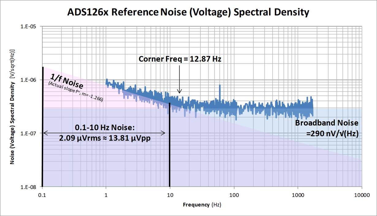
    Is there any data on the noise of the internal reference ads1262? Or just indirectly on the noise table (page 26 of Table1. ADC1Noise)? For now, temporarily, I'm using it.

    At 2.5 sps, the Sinc4 filter, gain 1 v/v, the simplest averaging over 20 measurements gives an “average” noise of + -150 nV peak to peak. I’m trying to find and remove who makes noise.

  • Hi Boris,

    We did measure the noise spectral density of the ADS1262's internal reference on one device, and this was the result:

    Table 1 data was acquired by shorting the inputs to the ADC, so reference noise is effectively removed from these measurements.

    I wrote up a blog post on this topic, describing how reference noise is modulated by the amplitude of the input signal: https://e2e.ti.com/blogs_/archives/b/precisionhub/archive/2015/12/11/the-impact-of-voltage-reference-noise-on-delta-sigma-adc-resolution

  • Interesting. This picture is from your measurements or maybe there are available documents with such measurements? For pga, current noise of input diodes and etc.

  • Hi Boris,

    Yes, this was a measurement I did on the bench. Unfortunately, I don't have any additional documentation I can point you to.

    For things like PGA, input diode current noise, there isn't a great way of decoupling and measuring each of these possible noise sources separately, so the best you can practically do is look at the combined noise performance of all of these sources from Table 1 and try to replicate it...

    Have you tried shorting the inputs to the ADS1262, measuring the noise performance, and then comparing the results to Table 1? Once, you've done that, try shorting the inputs of your external amplifier/signal conditioning and see if the noise degrades. That's generally how I do about trying to locate the main noise contributors.

  • I will prepare measurement data and compare. For the case of an internal reference source, external (for example, Ltc6655, as one of the lowest nois), with the ADC input shorted, the analog power supply has a noise of no more than 0.8 mV.

  • Noise with an internal reference source is as specified in the documents. When connecting an external reference source (output + -2.5 volts), a problem occurs. ADC bipolar supply voltage avdd +2.5 volts, avss -2.5 volts. Connecting an external reference source to the terminals AIN5 -2.5 volts, AIN4 +2.5 volts. PGA is disabled. Reference source LTC6655-2.5, inverting buffer on op177. When operating from an internal reference source, LSB ~ 1.164 nV (5 (FSR) / 2 ^ 32), from an external reference source LSB is ~ 2.382 nV. As if it became either FSR = 10 volts or LSB = FSR / 2 ^ 31. Why is that? The documentation says that the absolute value FSR = + REF - (-REF) is considered.

  • Last question not valid, ignore it. Sorry.)