Hi.
http://www.ti.com/lit/ds/symlink/ads131a02.pdf
I have some problems with this ADC:
1. High noise while inputs are shorted (diffrerence ~1200 adc points, VREF = 4 V, so noise is about 500uV in 24bit resolution)
2. SPI frame error: F_FRAME in STAT_S register is set after I done all initialization and truing to get data.
My setup:
AVCC 5V
DVCC 3.3V
VREF 4V - internal used
M0 - DVCC
M1 - DVCC
M2 - GND
So its Asynchronous interrupt mode, 32 bit SPI word size, Hamming code word validation off.
My intialization steps:
1. set RESET pin high
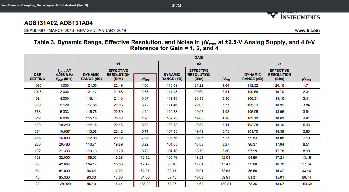
2. read 0x00 register to obtain 0xFF02 answer:
3. Unlock ADC(0x0655)
4. At this stage I can configure ADC already, but I made read of all registers.
For example, reading STAT_1: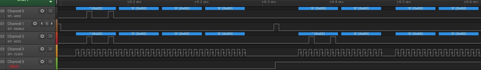
As you can see, all faults bits are clear.
Futher register readings gives me next:
STAT_P - 0x00
STAT_N - 0x00
STAT_S - 0x00 (no SPI errors!)
ERROR_CNT - 0x00
STAT_M2 - 0x05 (0000 0101b - setup as I described above)
A_SYS_CFG - 0x60
D_SYS_CFG - 0x3C
CLK1 - 0x08
CLK2 - 0x86
ADC_ENA - 0x00
ADC1 - 0x00
ADC2 - 0x00
Pretty same as it should be by default.
5. Now I set CLK2 to E0 (1110 0000b)
So
- fMOD = fICLK / 14
- fDATA = fMOD / 4096
Making delay 260MS and readback this register to confirm setup.
6. Set A_SYS_CFG to 0x78 (0111 1000b)
So
- REFP is set to 4.0 V
- Internal reference voltage enabled and selected
Making delay 260MS and readback this register to confirm setup.
7. Set ADC_ENA to 0x0F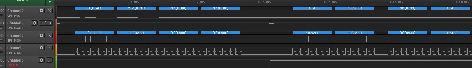
Responce differs from datasheet - it should be 0x0F, but I receive 0x03.
I suppose its because I'm using 2channel device (so 0x03 = 0000 0011b), but correct me if I'm wrong.
Making delay 260MS and readback this register to confirm setup (its again 0x03).
8. Send WAKEUP: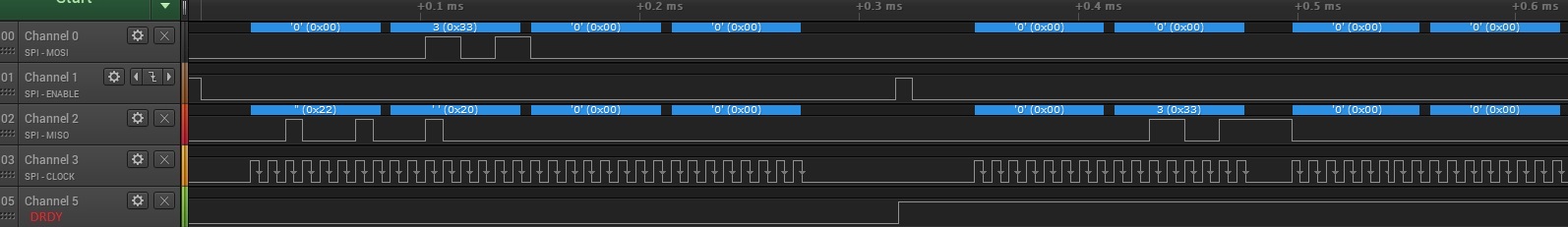
Making delay 260MS.
9. Send LOCK command: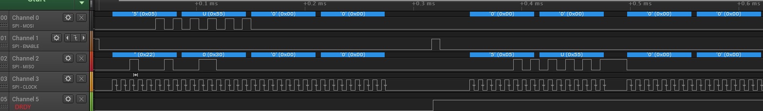
Making 300MS delay after this.
10. Polling RDRY pin: when it go LOW, I'm start sending NULL command:
Now error 0x30 appeared (it says SPI error), I've read additionaly STAT_S register and it gives 0x01:
Not enough SCLKs are sent per frame
Moreover, my channels are shorted and results are:
0x000739 = 1849 for CH1
0x0004F0 = 1264 for CH2
Why its so differs?
Here is some others samples:
0x000736 = 1846 for CH1
0x0004EE = 1258 for CH2
0x000731 = 1841 for CH1
0x0004EB = 1259 for CH2
Hope for assistance, thanks!
Regards