This thread has been locked.

If you have a related question, please click the "Ask a related question" button in the top right corner. The newly created question will be automatically linked to this question.

CCS/DAC81416EVM: Connecting the MSP430F5529 with the DAC81416 through SPI

Part Number: DAC81416EVM

Tool/software: Code Composer Studio

Hello, 

I am currently trying to connect the MSP430F5529 with the DAC81416 through SPI. I want to be able to read and write to the registers in the DAC, as a test I have made a simple program that reads the device id (0x29C0) and compares it to a constant. If the value read is correct, then the led (P1.0) on the MSP toggles indefinitely. I am having trouble getting SPI to work correctly.  Here are the steps I am taking and some sample code I have prepared.

  1. set CS pin low
  2. spi_write: 0x81, 0xff, 0xff
  3. set CS pin high
  4. delay cycles. maybe needed, maybe not.
  5. set CS pin low
  6. write 3 dummy byes
  7. read the response into a buffer
  8. set CS pin high
  9. return (output[1]<<8) | (output[2]);// [0] = register echo, [1] = low part bits 16-8, [2] = bits 7-0

attached is my code, note SPI_POLLING is defined with -D as a global defined this is the non-interrupt state machine way of using the spi driver for lower level communication.

Thank you, 

Andres

spi.h

  • 8400.spi.c
    #include <msp430.h>
    #include <spi.h>
    #include <intrinsics.h>
    #include <stdint.h>
    
    void spi_init(void)
    {
        P3SEL |= BIT3 | BIT4;
        P2SEL |= BIT7;
        spi_disable();
        //CTL1 SMCLK
        UCA0CTL1 |= UCSSEL_2;
        /* CTL0 - master mode
         *      - 8 bit char length
         *      - CS inactive state high
         *      - 3 pin spi
         *      - synchronous mode
         */
        UCA0CTL0 |=  UCMST
                    | UCSYNC
                    | UCMSB
                    | UCCKPH
                    ;
        UCA0BR0 = 0x02;
        UCA0BR1 = 0x00;
        UCA0MCTL = 0;
        spi_enable();
    #ifndef SPI_POLLING
        spi_enable_interrupt(UCRXIE);
    #endif
        SPI_SLAVE_CS_DIR |= SPI_SLAVE_CS_PIN;
        SPI_SLAVE_CS_OUT |= SPI_SLAVE_CS_PIN;
    }
    
    void spi_enable(void)
    {
        UCA0CTL1 &= ~(UCSWRST);
    }
    
    void spi_disable(void)
    {
        UCA0CTL1 |= UCSWRST;
    }
    
    uint8_t spi_is_busy(void)
    {
        return UCA0STAT & UCBUSY;
    }
    
    uint8_t spi_is_not_busy(void)
    {
        return !spi_is_busy();
    }
    
    void spi_enable_interrupt(uint8_t spi_interrupt_type)
    {
        UCA0IE |= spi_interrupt_type;
    }
    
    void spi_disable_interrupt(uint8_t spi_interrupt_type)
    {
        UCA0IE &= ~(spi_interrupt_type);
    }
    
    uint8_t spi_get_interrupt_status(uint8_t spi_interrupt_type)
    {
        return UCA0IFG & spi_interrupt_type;
    }
    
    void spi_clear_interrupt(uint8_t spi_interrupt_type)
    {
        UCA0IFG &= ~(spi_interrupt_type);
    }
    
    #ifndef SPI_POLLING
    typedef enum spi_mode{
        IDLE_MODE,
        TX_REG_ADDRESS_MODE,
        RX_REG_ADDRESS_MODE,
        TX_DATA_MODE,
        RX_DATA_MODE,
        TIMEOUT_MODE
    } spi_mode_t;
    
    spi_mode_t current_mode = IDLE_MODE;
    uint8_t tx_reg_addr = 0;
    uint8_t tx_buffer[SPI_MAX_BUFF_SIZE] = {0};
    uint8_t tx_buff_idx = 0;
    uint8_t tx_count = 0;
    
    uint8_t rx_buffer[SPI_MAX_BUFF_SIZE] = {0};
    uint8_t rx_buff_idx = 0;
    uint8_t rx_count = 0;
    
    void copy(uint8_t *src, uint8_t *dst, uint8_t size)
    {
        uint8_t idx;
        for(idx = 0; idx < size; idx++)
            dst[idx] = src[idx];
    }
    
    void spi_write(uint8_t reg, uint8_t *bytes, uint8_t size)
    {
        current_mode = TX_REG_ADDRESS_MODE;
        copy(bytes, tx_buffer, size);
        tx_reg_addr = reg;
        tx_count = size;
        rx_count = 0;
        rx_buff_idx = 0;
        tx_buff_idx = 0;
    
        SPI_SLAVE_CS_OUT &= ~(SPI_SLAVE_CS_PIN);
        spi_write_byte(tx_reg_addr);
        __bis_SR_register(LPM0_bits + GIE);
        SPI_SLAVE_CS_OUT |= SPI_SLAVE_CS_PIN;
    }
    
    void spi_read(uint8_t reg, uint8_t size)
    {
        current_mode = TX_REG_ADDRESS_MODE;
        tx_reg_addr = reg;
        rx_count = size;
        tx_count = 0;
        rx_buff_idx = 0;
        tx_buff_idx = 0;
    
        SPI_SLAVE_CS_OUT &= ~(SPI_SLAVE_CS_PIN);
        spi_write_byte(tx_reg_addr);
    
        __bis_SR_register(LPM0_bits + GIE);
    
        SPI_SLAVE_CS_OUT |= SPI_SLAVE_CS_PIN;
    }
    
    #if defined(__TI_COMPILER_VERSION__) || defined(__IAR_SYSTEMS_ICC__)
    #pragma vector=USCI_A0_VECTOR
    
    __interrupt void USCI_A0_ISR(void)
    
    #elif defined(__GNUC__)
    void __attribute__ ((interrupt(USCI_A0_VECTOR))) USCI_A0_ISR (void)
    #else
    #error Compiler not supported!
    #endif
    
    {
      uint8_t uca0_rx_byte = 0;
      switch(__even_in_range(UCA0IV,4))
      {
        case 0:break;                             // Vector 0 - no interrupt
        case 2:                                   // Vector 2 - RXIFG
            uca0_rx_byte = UCA0RXBUF;
            switch (current_mode)
            {
                case TX_REG_ADDRESS_MODE:
                    if (rx_count)
                    {
                        current_mode = RX_DATA_MODE;   // Need to start receiving now
                        //Send DUMMY To Start
                        __delay_cycles(50);
                        spi_write_byte(DUMMY);
                    }
                    else
                    {
                        current_mode = TX_DATA_MODE;        // Continue to transmision with the data in Transmit Buffer
                        //Send First
                        spi_write_byte(tx_buffer[tx_buff_idx++]);
                        tx_count--;
                    }
                    break;
    
                case TX_DATA_MODE:
                    if (tx_count)
                    {
                      spi_write_byte(tx_buffer[tx_buff_idx++]);
                      tx_count--;
                    }
                    else
                    {
                      //Done with transmission
                      current_mode = IDLE_MODE;
                      __bic_SR_register_on_exit(CPUOFF);      // Exit LPM0
                    }
                    break;
    
                case RX_DATA_MODE:
                    if (rx_count)
                    {
                        rx_buffer[rx_buff_idx++] = uca0_rx_byte;
                        //Transmit a DUMMY
                        rx_count--;
                    }
                    if (rx_count == 0)
                    {
                        current_mode = IDLE_MODE;
                        __bic_SR_register_on_exit(CPUOFF);      // Exit LPM0
                    }
                    else
                    {
                        spi_write_byte(DUMMY);
                    }
                    break;
    
                default:
                    __no_operation();
                    break;
            }
            __delay_cycles(60);
            break;
        case 4:break;                             // Vector 4 - TXIFG
        default: break;
      }
    }
    
    #else
    
    void spi_write_byte(uint8_t byte)
    {
        while (!spi_get_interrupt_status(UCTXIFG));
        UCA0TXBUF = byte;
    }
    
    void spi_write_bytes(uint8_t *bytes, uint8_t size)
    {
        SPI_SLAVE_CS_OUT &= ~(SPI_SLAVE_CS_PIN);
        uint8_t i;
        volatile uint8_t dump;
        for (i = 0; i < size; i++ )
        {
            spi_write_byte(bytes[i]);
            dump = spi_read_byte();
        }
        SPI_SLAVE_CS_OUT |= SPI_SLAVE_CS_PIN;
    }
    
    uint8_t spi_read_byte(void)
    {
        spi_write_byte(DUMMY);
        while (!spi_get_interrupt_status(UCRXIFG));
        return UCA0RXBUF;
    }
    
    void spi_read_bytes(uint8_t *bytes, uint8_t size)
    {
        uint8_t i;
        SPI_SLAVE_CS_OUT &= ~(SPI_SLAVE_CS_PIN);
        for (i = 0; i < size; i++ )
        {
            bytes[i] = spi_read_byte();
        }
        SPI_SLAVE_CS_OUT |= SPI_SLAVE_CS_PIN;
    }
    uint8_t spi_transfer(uint8_t byte_to_send)
    {
        SPI_SLAVE_CS_OUT &= ~(SPI_SLAVE_CS_PIN);
        UCA0TXBUF = byte_to_send;
        while (!spi_get_interrupt_status(UCRXIFG) );
        uint8_t byte_received = UCA0RXBUF;
        SPI_SLAVE_CS_OUT |= SPI_SLAVE_CS_PIN;
        return byte_received;
    }
    
    uint16_t spi_transfer16(uint16_t word_to_send)
    {
        uint16_t word_received;
        uint8_t *word_to_receive_as_bytes = (uint8_t *)&word_received, *word_to_send_as_bytes = (uint8_t *)&word_to_send;
        SPI_SLAVE_CS_OUT &= ~(SPI_SLAVE_CS_PIN);
        UCA0TXBUF = word_to_send_as_bytes[1];
        while ( !spi_get_interrupt_status(UCRXIFG) );
        word_to_receive_as_bytes[1] = UCA0RXBUF;
        UCA0TXBUF = word_to_send_as_bytes[0];
        while ( !spi_get_interrupt_status(UCRXIFG) );
        word_to_receive_as_bytes[0] = UCA0RXBUF;
        SPI_SLAVE_CS_OUT |= SPI_SLAVE_CS_PIN;
        return word_received;
    }
    #endif
    
    DAC81416.c
    #include <msp430.h>
    #include <spi.h>
    #include <DAC81416.h>
    #include <stdint.h>
    
    #ifndef SPI_POLLING
    extern uint8_t rx_buffer[SPI_MAX_BUFF_SIZE];
    #endif
    
    void DAC81416_init(void)
    {
       spi_init();
       DAC81416_write_register(SPICONFIG, SDO_EN);
    }
    
    void DAC81416_write_register(uint8_t reg_to_write, uint16_t config)
    {
    #ifdef SPI_POLLING
        uint8_t send[3];
        send[0] = reg_to_write;
        send[1] = (config >> 8);
        send[2] = config & 0xff;
        spi_write_bytes(send, 0x03);
    #else
        DAC81416_data_t command;
        command.data = config;
        spi_write(reg_to_write, command.data_serial, 0x02);
    #endif
    }
    
    uint16_t DAC81416_read_register(uint8_t reg_to_read)
    {
        uint8_t rtr = READ_BIT | reg_to_read;
    #ifdef SPI_POLLING
        uint8_t arr_in[3] = {rtr, DUMMY, DUMMY};
        uint8_t arr_out[3];
        spi_write_bytes(arr_in, 0x03);
        __delay_cycles(5);
        spi_read_bytes(arr_out, 0x03);
        uint16_t o = (arr_out[2] << 8) | arr_out[1];
        return o;
    #else
        spi_read(rtr, 0x03);
        return (rx_buffer[0] | (rx_buffer[1] << 8));
    #endif
    
    
    }
    
    //read out registers
    uint16_t DAC81416_get_device_id(void)
    {
        return DAC81416_read_register(DEVICEID);
    }
    
    uint16_t DAC81416_get_status(void)
    {
        return DAC81416_read_register(STATUS);
    }
    
    uint16_t DAC81416_get_dac_data(uint8_t dac)
    {
        return DAC81416_read_register(dac) & 0xFFFF;
    }
    
    DAC81416.h
    5658.main.c
    #include <msp430.h>
    #include "DAC81416.h"
    uint16_t device_id;
    int main(void)
    {
        //simple test to verify that the dac driver is working correctly
    	WDTCTL = WDTPW | WDTHOLD;
    	DAC81416_init();
    	P1DIR |= BIT0;
    	while(1)
    	{
    	    device_id = DAC81416_get_device_id();
    	    if( DEVICE_ID_VAL == (device_id & DEVICE_ID_MSK ))
    	    {
    	        while(1)
    	        {
    	            P1OUT ^= BIT0; // toggle LED
    	            __delay_cycles(100);
    	        }
    	    }
    	    __delay_cycles(100);//retry to see waveform on oscilliscope
    	}
    
    	return 0;
    }
    
    DAC81416.h

  • Andres,

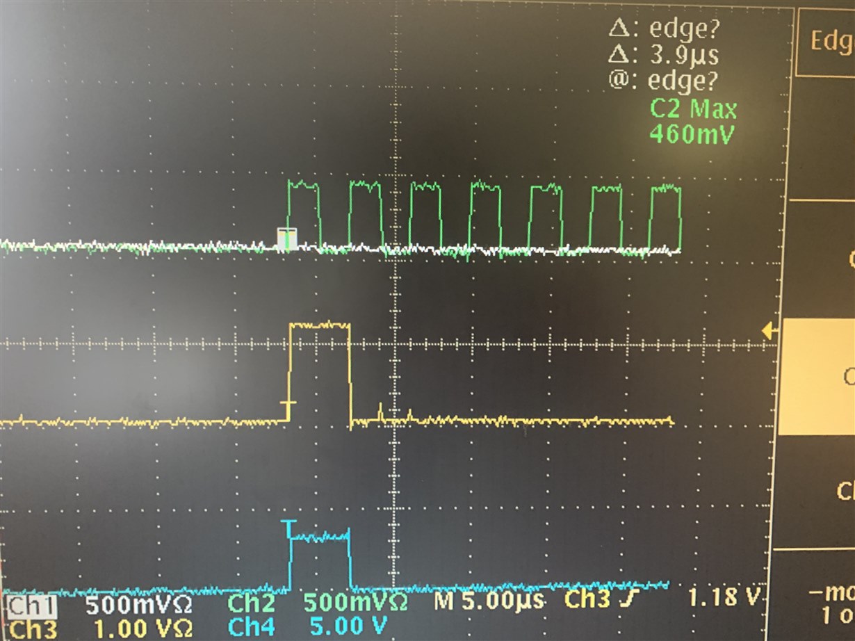
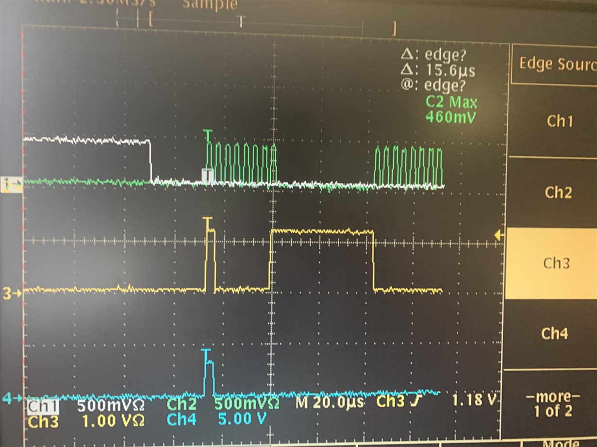
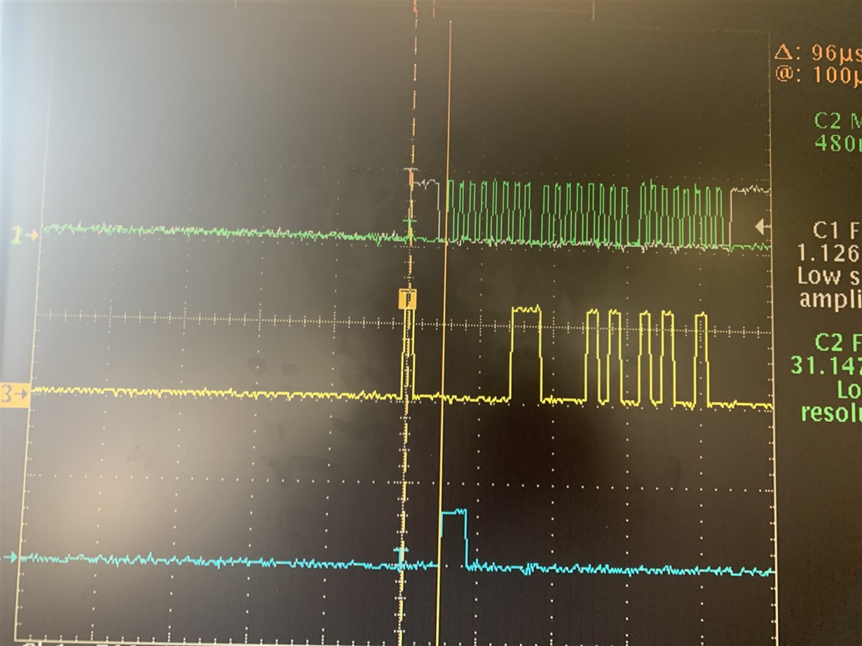
    Could you please share a capture of the actual physical bus activity so we can verify the integrity / timing of these signals?

  • Channel 1 is the CS line

    Channel 2 the clock

    Channel 3 is SDI/MOSI

    Channel 4 is SDO/MISO

    From what I understand bit23 is read, A (the register is 0x01(device id) and the rest is just 0, then on readout (part after CS goes high)  it can be any dac command so I write a noop to the DAC 0x00, 0x00, 0x00, however instead of reading 0x29C I read 0x04

    -Andres

  • Hi Andres,

    I think it is critical that you confirm the edges of the SPI signal (ensuring the master is updating the output on the rising edge, not the falling edge).  Unfortunately, this capture does not have that resolution.  Can you adjust the time scale to better capture this? You could also reduce your clock speed.

    Thanks,

    Paul

  • Hi Paul,

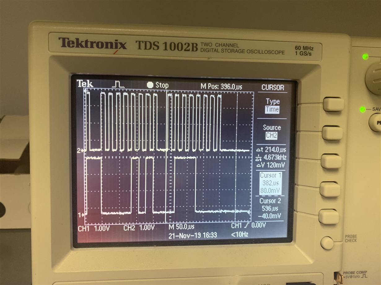
    I halved the clock speed (changed UCA0BR0 to 0x04 instead of 0x02) and scaled in, here are 2 images, of the first command (0x81, 0x00, 0x00). the second command is a noop (0x00, 0x00, 0x00).

    interesting note: I connected the USB2ANY and the DACEVM software to spy on proper communication between an MCU and the DAC and found that there was about a 15ms delay where CS is high between the write cycle and the read out cycle, I didn't see this on the timing diagram above. 

    - Andres

  • Hi Andres,

    Two things:

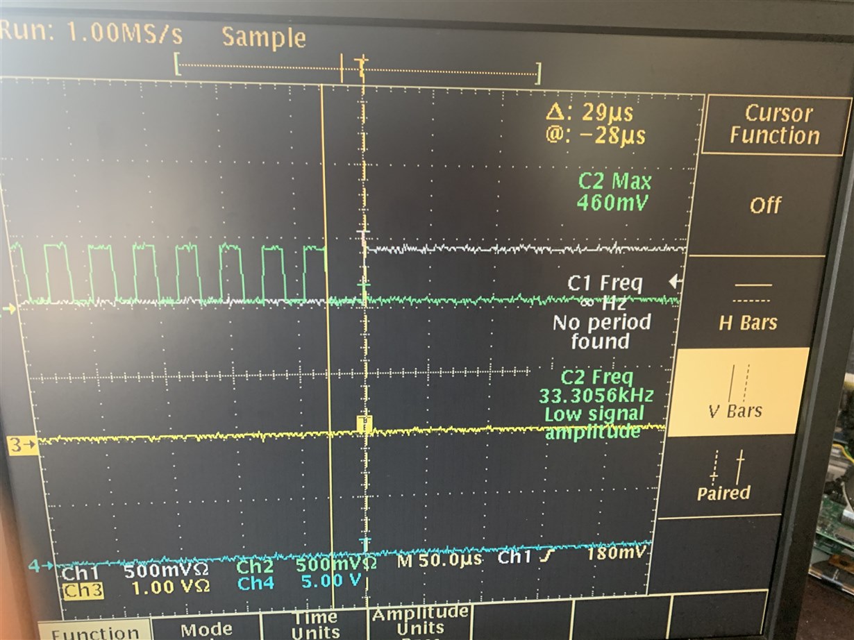
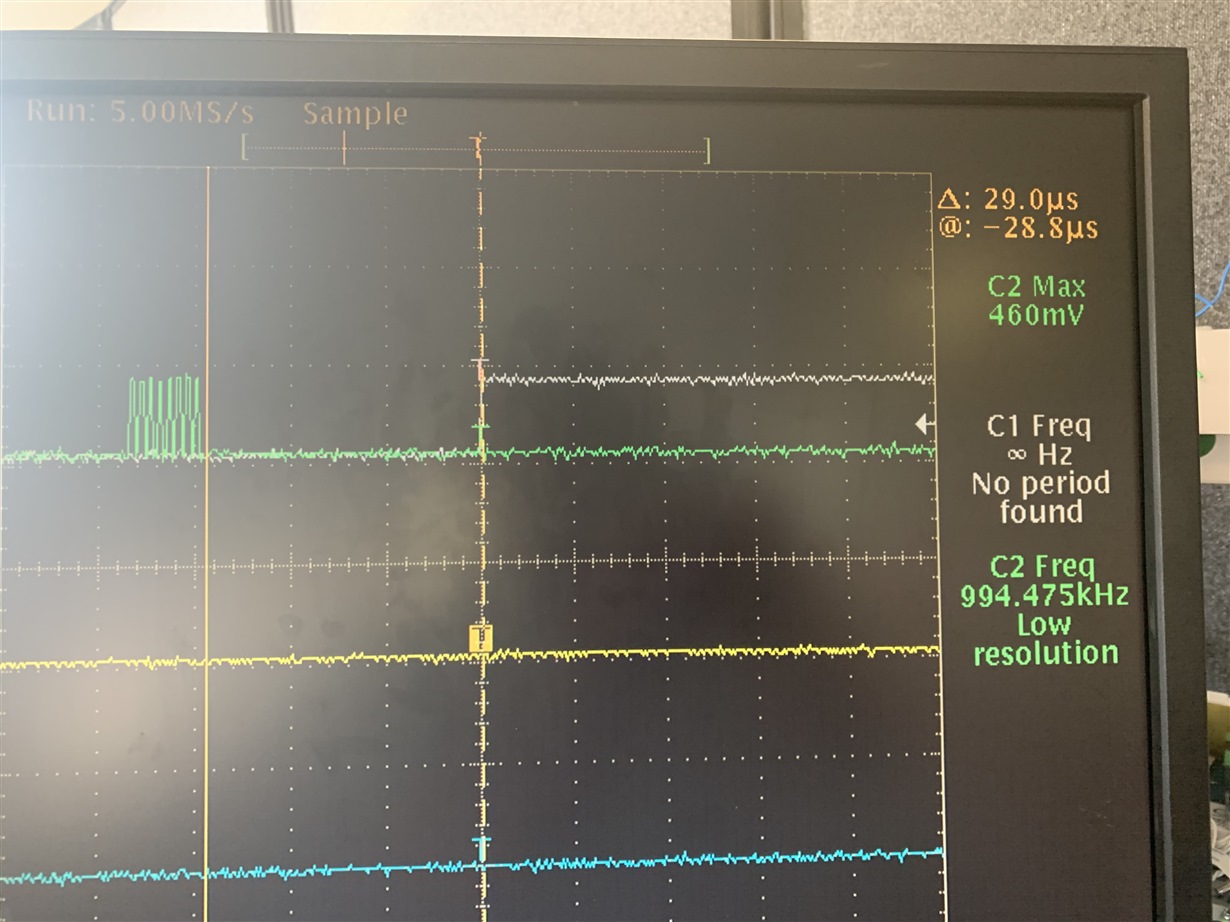
    1. It is not clear in the images you shared if CS is held low for the final clock pulse.  Can you confirm this?  Specifically, is tCSH is being provided?

    2. SDO should be enabled by default, but it is worth trying.  Can you write to the SPI config register to ensure that the SDO-EN bit is set?

    Write (0x03, 0x0AA4)

    Thanks,
    Paul

  • Hi Paul, 

    tCSH in the datasheet has a minimum time of 5-10 ns depending on Vio, in the first picture below it is clearly well above that at 28 us.

    Even running sclk at 1Mhz (CH2 @999Khz) the delay is still in the microsecond range

    Picture 3 is the write commad to the SPICONFIG register with 0x0AA4.

    Thanks,

    Andres

  • Andres,

    I apologize for the lack of updates on this thread. This one has slipped through the cracks between Paul and my support. Have you made any progress on the issue since your last post?

  • Hi Kevin,

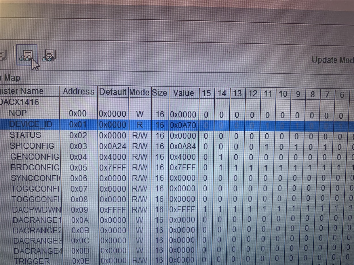
    I have made a decent amount of progress and noticed something very interesting. I have verified that I can write valid data to the dac. I enabled multiple dac outputs and wrote voltages to them using my software and everything seems to be in line with the proper voltages being outputted, however, I am still unable to read out valid data. I currently have 2 dacs at my disposal and have run my program on both and seen valid results on both. When reading out from the device id register however I noticed with one, dac I was reading 0x0A70 and while I didn't document the other, it was giving me back something along the lines of 0xFFEF. Interestingly 0x0A70 is 0x29C0 right-shifted twice. This readout was done using the standard software that comes with the dac and was transmitted using the USB2ANY programmer. Again, I was able to write valid data to both dacs with both the software provided by TI and my own, however for the purposes of my application, I must be able the device id from the dac and validate that I have a proper connection established. 

    Let me know what you think.

    Best,

    Andres 

  • Hi Andres,

    Thanks for being patient with the delays.  The holidays really slowed things down as most of the team was out of office.

    In regards to the 0x0A70 value in the Device-ID register - this is correct.  It is a bit confusing as in our register map we usually use a "field" method to describe register sub-functions.

    What we are trying to convey is that there are two fields in this register.  The first, DEVICEID, is 14 bits wide.  The second, VERSIONID, is 2 bits wide.

    When you consider the 14-bit value and assume the default is right-justified then the field's value is 0x29C (14-bit).  When you put that in the register, that field now occupies the left-most 14 bits.  So the data would look left-shifted by 2 bits.

    Now we need to dig into the other DAC reading back 0xFFEF.  Is that repeatible?

    Thanks,

    Paul