This thread has been locked.

If you have a related question, please click the "Ask a related question" button in the top right corner. The newly created question will be automatically linked to this question.

DAC8771: Behavior when miss-wiring

Part Number: DAC8771

Hi team,

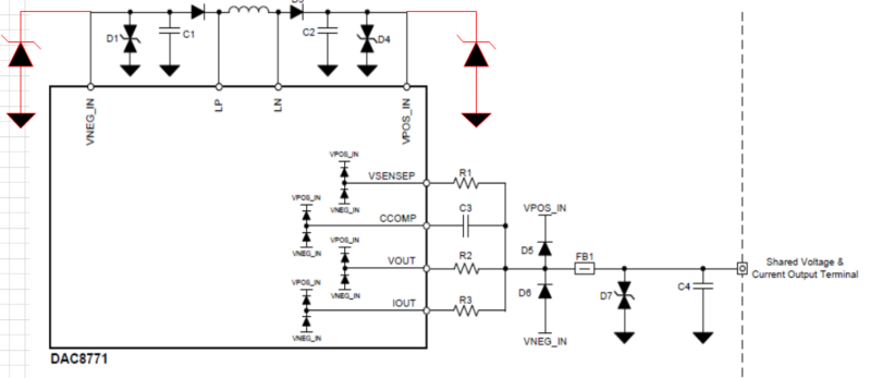
My customer has concern about there is as possibility for miss-wiring by end user.

In the worst, -32V will apply on Vout/Iout. Abs max is -20V so the device may get damage.

1. Could you tell me which parts will get damage when applying -32V?

2. How to behave the device when applying the unexpected voltage? some fault may indicate?

3. Would it be possible to share the actual value  abs max value of the Vout/Iout?

Regards,

Yoshi

  • Yoshi,

    How is the device being used? Is the negative DC/DC rail active or is VNEG grounded?

    The absolute maximum table already defines the absolute maximum voltages allowed at VOUT / IOUT. VNEG - 0.3V minimum and VPOS + 0.3V maximum.

  • Hi Kevin,

    Thanks for checking.

    Negative DCDC is active.

    The customer need to confirm how the device get damage when apply the -32V.

    I understood absolute max is mentioned in the datasheet. Do you have additional data such as the device can withstand above maximum voltage for few msec?

    Regards,

    Yoshi

  • Yoshi,

    It is always hard to comment on "short-term" violations of the absolute maximum ratings table. Mostly this depends on the current sinking capability of the -32V and whether there are any pass elements in between the -32V and the VOUT/IOUT pins.

    This is for two reasons:

    1. When we violate the absolute maximum ratings table for VOUT or IOUT (not the VPOS/VNEG relationship) ESD cells inside the device which are basically clamp to rail diodes will become forward biased and begin to conduct. They are not designed for in-circuit, or in-system, conduction and in these cases the main concern is how much forward current they conduct. For DAC8771 we would really like to keep this <100mA or so (this is just an estimate, nothing that we really characterize).
    2. When these ESD cells are conducting you will be charging the DC/DC storage capacitor, in this case the VNEG capacitor. If the current is limited sufficiently such that the storage capacitor is not fully charged to -32V, or otherwise enough to violate the absolute maximum ratings table, we will probably be good. Otherwise, the DC/DC doesn't really have any capability to "fight" this charging to save the absolute maximum ratings table.

    If the threshold is exceeded it is possible that other another internal protection circuit, which is essentially an SCR, would turn on and begin conducting. Until the current through the SCR goes below the holding current it will not stop conducting, which would probably only happen if power were completely removed from the system. Typically the SCR does not engage until a value higher than the absolute maximum rating, but -32V does pretty significantly violate the table so I feel like it could be likely.

    I would also recommend having a TVS diode on both VPOS and VNEG as is included in our reference material. Having a TVS diode with breakdown voltage ~18V on VNEG would help regulate how much the VNEG storage capacitor is charged, especially well if the current is limited as I mentioned in points 1) and 2).

  • Hi Kevin,

    Thanks for your comment.

    To limit the current, the customer need to use external circuit on. Is my understanding correct?

    Also, could you tell me how to connect the additional TVS diode on VPOS and VNEG? Could you check whether attached picture correct or not.

    Regards,

    Yoshi

  • Yoshi,

    Masayoshi Takahashi said:
    To limit the current, the customer need to use external circuit on. Is my understanding correct?

    Yes - to some extent this is already present in R1, R2, and R3 in the diagram you have copied. In the reference design material these are 15 ohm resistors, which probably will not be sufficient to indefinitely protect against this miswiring case. It depends on D7 and D5/D6 and where they will effectively clamp the voltage at the shared VOUT/IOUT node. FB1 will not be very effective against a DC condition - so if they can accept some loss of accuracy associated with replacing FB1 with another resistor, that would be beneficial to increase the effectiveness of D5/D6.

    Masayoshi Takahashi said:
    Also, could you tell me how to connect the additional TVS diode on VPOS and VNEG? Could you check whether attached picture correct or not.

    D1 and D4 are bidirectional TVS diodes which represent what I was suggesting. You do not need to add any extra diodes. The reference design material assumes a sort of generic use case - but in this case it could be helpful to choose a TVS diode for VNEG that breaks down closer to 18V or perhaps even less based on their loading conditions. VNEG is set to -15V by default for VOUT mode, in IOUT mode the most negative value on VNEG is dependent on the load impedance on IOUT.

  • Hi Kevin,

    Thanks for telling me.

    Would it be possible to calculate R1, R2 and R3 resistor to limit the current for -32V over voltage?

    When the customer change the FB1 to resistor, then the customer calculated R1 and additional resistor.

    The value is around 1.2k ohm (current limit is 0.022A)

    Is this value seems high compare to reference design. Can the customer use 1.2 kohm? The customer wondering if the device can work accurately.

    Regards,

    Yoshi

  • Yoshi,

    I don't really follow how this calculation was performed. Most likely D5, D6, and D7 are going to limit the voltage at VOUT/IOUT to something much closer to VNEG than -32V so a smaller value should be reasonable. We just need to know what diodes they are using in these positions and how much current to expect from the -32V source to get an idea of where each element is going to clamp. We would start with D7, then use some reasonable resistor value in place of FB1 to help out D5 / D6 then, ideally, a small resistance inside of the feedback network.

  • Hi Kevin,

    I understand smaller value is reasonable. Do you think is there any problem by using 1.2k ohm resistor?

    Regards,

    Yoshi

  • Yoshi,

    I guess it depends to some extent where we are discussing placing this resistor - but yes in virtually every location it will cause problems.

    For IOUT having this series impedance between the IOUT pin and the load will eat into the maximum allowable load. 20mA for example into the 1.2kOhm load will already require a 26V VPOS. VPOS maximum is 33V. So there would be headroom only for 350 ohm loads.

    For VOUT, this resistor outside of the feedback loop would create a voltage divider with the load, which is typically 1kOhm minimum - so a significant divider. If it is within the feedback network, it is starting to become a large enough value to be comparable to the internal feedback resistors, so it would begin to introduce a gain error.

    We want to try our best to optimize the circuit with the smallest resistors possible. To do that, we need details about their chosen diodes.