This thread has been locked.

If you have a related question, please click the "Ask a related question" button in the top right corner. The newly created question will be automatically linked to this question.

DAC088S085: SPI communication with DAC088S085 and daisychianing

Part Number: DAC088S085

To whom it may concern,

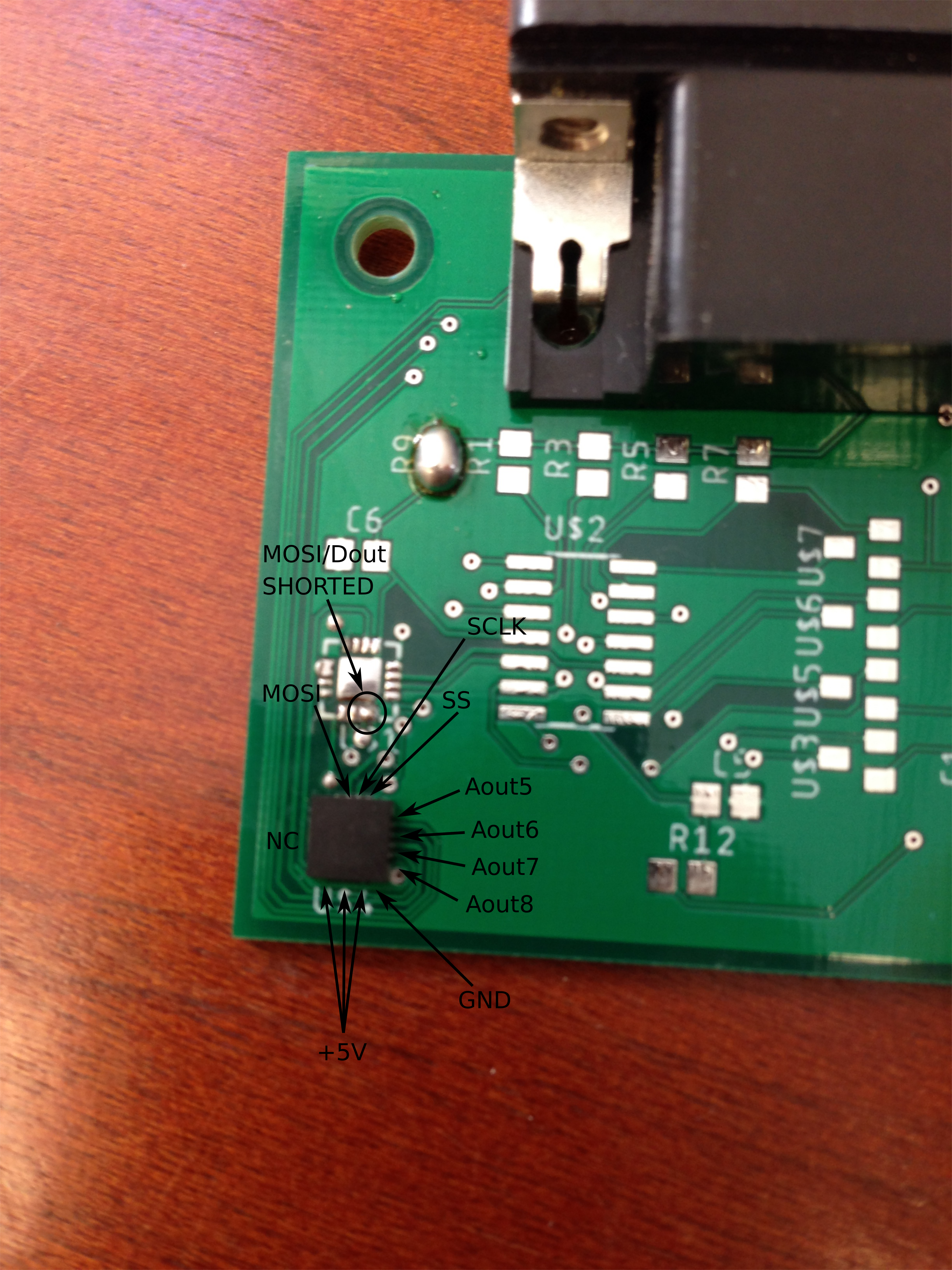
I'm trying to control two daisychained DAC088S085 via SPI protocol. Right now on a PCB I only connected one device with Va =Vref1=5V, MOSI, CLK and SS, the analog outs are not loaded. Here the specific of my communication protocol: SPIMODE1, MSBFIRST, fclock = 14MHz, CS active LOW.

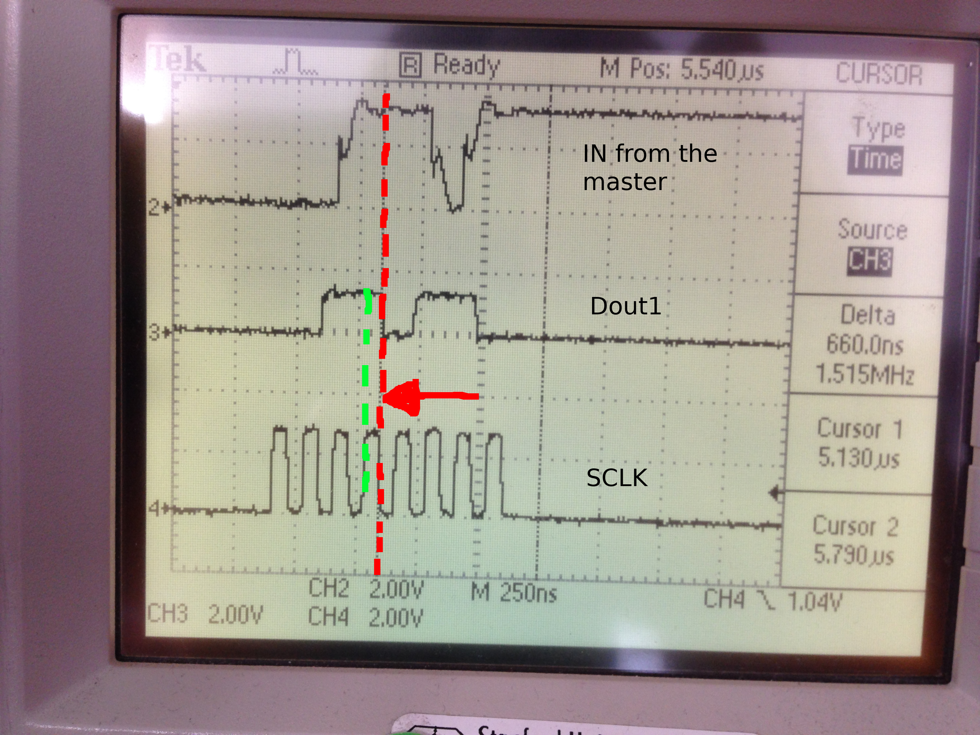
As a test, I would like to see the analog output changing according to my code and see Dout1, for testing the daisychain method. After I sent to the device the 1001000000000000, to switch it to WTM mode, I would expect the analog outs to change as I send the commands, but I don't see the voltage on the outs changing. Furthermore Dout1 appears to be somewhat out of sync (more clear explanation in the pictures below). What am I doing wrong?

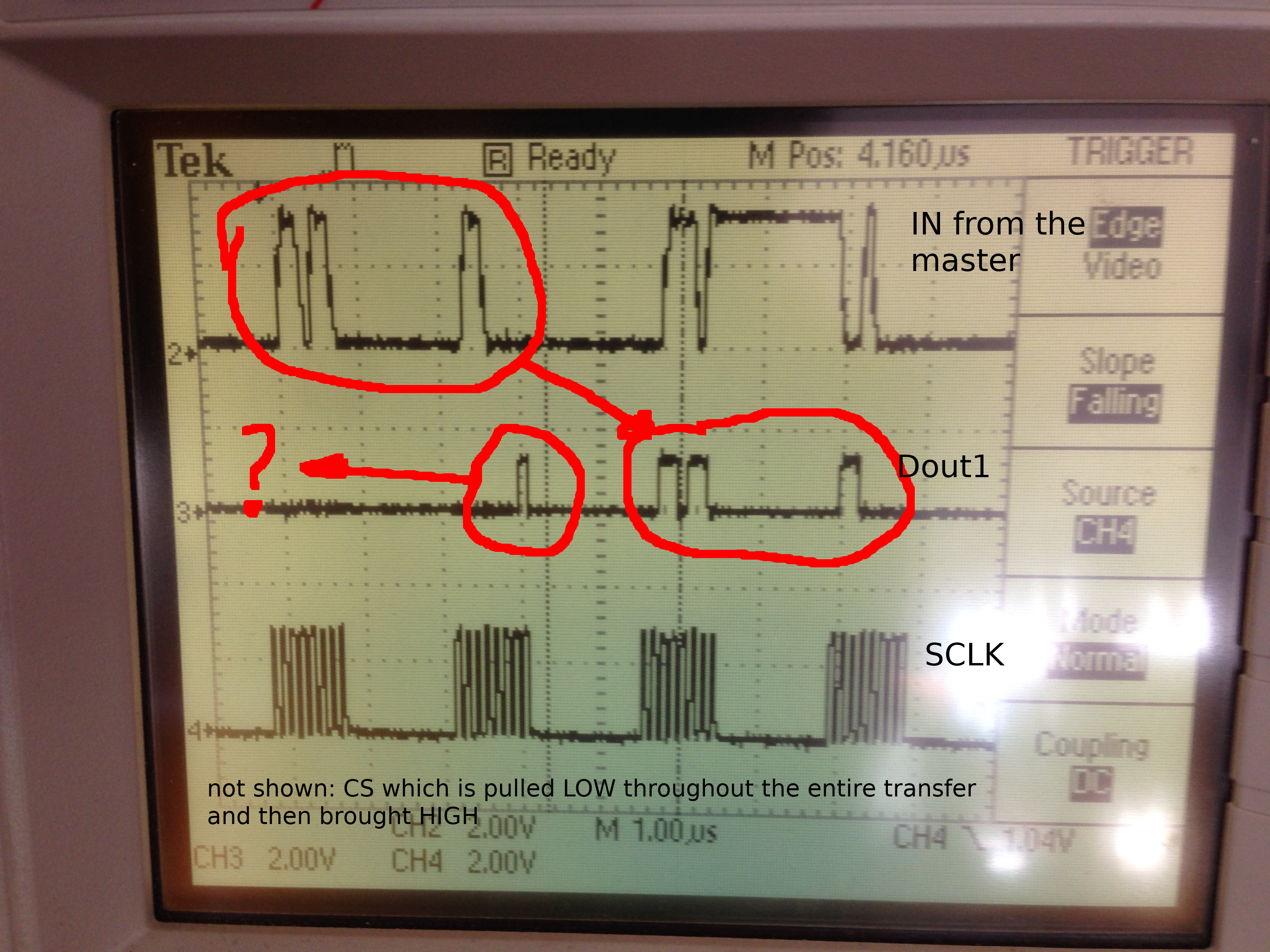
In this image I'm sending to the VoutD of DAC1 the number 178 (16 bits 00111011 00100000) and to VoutD of DAC2 the number 102 (00110110 01100000). Looking at the Dout1 I can see it copies the first input and sends it to the second 16-bits block instruction as expected, apart from one bit (in the first 16 block, highlighted with a question mark in the picture) and the Dout1 high value less than 2V.  Are these normal? Moreover what is more confusing is shown in this second picture, which is simply a zoomed in version of the third 8-bits instruction. It is possible to see how the in from the master is synced correctly to the falling edge of the clock (red dashed line), while Dout1 seems to be synced with the rising edge (green dashed line), what is going on? Any help would be appreciated

  • EDIT: Dout1 HIGH value is correct to 5V, in those images the scope simply terminated at 50ohms, the other problems still remain

  • Hi Jacopo,

    I am concerned about the Master-out-slave-in line that you show in your plots.  It does not have clean transitions and that could cause the device to be latching the data incorrectly. 

    Can you share a schematic of your design?

    A good step to debug this would be to first just try to write to the first DAC (only send 16-bit frames) and lets see if we can get that one to update.

    Thanks,

    Paul

  • Any updates?

  • hi Paul_Frost,

    thank you for your reply and sorry for my late reply. The MISO was a problem of grounding, after cleaning it up a little bit it looks better, although I don't think that was particularly concerning since I could correctly see the Dout1 (it just appears shifted on the rising edge of the clock). Anyway I'm able to make work the two DACs independently (meaning whenever they are not daisychained), it was simply not soldered properly to the PCB (wqfn packaging). The problem remains when I daisychain the two, I see the first DAC (the one on top) pulling a lot a current, until it burns, while the second one (the one on the bottom) works fine.

    In the first picture you can see the just the first DAC with the pinout connection and I can control this one correctly (all the inputs are coming straight from the controller)

    In the second picture you can see the same for the second DAC, apart the fact that the MOSI pad and the DAISYCHAIN/Dout pad are shorted (this to communicate straight with the second DAC bypassing the first), also in this configuration I can control the outs.

    as I said, whenever I have on the board both (in this case MOSI and Dout are not shorted), I see the device on top burning while the one on the bottom is fine. Having them tested separately makes me think it's not a problem of the board. In the last picture you can see the layout of the board, SS, SCLK, MOSI and V+ are provided by the controller

    any insight would be helpful.

    Jacopo

  • Hi Jacopo,

    I am concerned that the footprint for the device is not correct. Is it possible that adjacent pins are being short or the thermal pad on the bottom is shorting some of the pins? 

    When I look a the exposed metal diagram, it seems incompatible with the land pattern you are showing.  Can you verify the dimensions of your footprint?

    Thanks,

    Paul