This thread has been locked.

If you have a related question, please click the "Ask a related question" button in the top right corner. The newly created question will be automatically linked to this question.

ADS54J60: Unequal probability of quantization bins

Part Number: ADS54J60

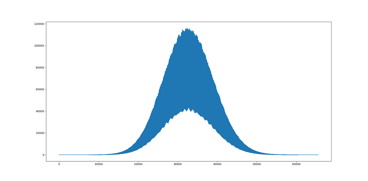
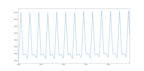
We have an ADS54J60 on an Abaco FMC120. We recorded Gaussian broadband noise (400 MHz bandwidth) with the 16 bit ADC from the ADS54J60 with a sampling rate of 1 GS/s. We then calculated the histogram by counting the occurrences of each of the 2**16 quantization levels. The result is shown below. The expected outcome is a Gaussian distribution. The measured outcome is that every fourth bin is about 2 to 3 times more probable than the adjacent 3 bins. DC offset was frozen for this measurement.

Histogram:

Zoom into the middle region:

Looking at the DC offset idle channel histogram when the DC offset correction is disabled, one of the peaks is much higher than the three others and shows a similarly strange pattern. According to the datasheet of the ADS54j60 the four peaks should be similar in nature (Figure 146). I'm not sure if this is related to the problem at hand.
ADC0 to ADC3 all behave the same.
Is this behavior expected? What is the reason for the behavior? Is this something which can be improved? It generates quite some problems for our application, possibly rendering the use of the ADS54J60 impossible.
Thank you very much for your help!
  • Tobias,

    For the most part, this is expected of the part. There are a couple of register writes that may improve this. Can you send your register settings?

    Regards,

    Jim

  • Dear Jim,

    I use the Abaco reference software for programming the registers. I wrote a script extracting the register values, please see below (the simplest was to loop through all register addresses, not only the used ones)

    Best regards,

    Tobias

    Master Page of Analog Bank

    0020 00
    0021 00
    0022 00
    0023 00
    0024 00
    0025 00
    0026 40
    0027 00
    0028 00
    0029 01
    002A 54
    002B 00
    002C 02
    002D E4
    002E BC
    002F 00
    0030 00
    0031 02
    0032 78
    0033 00
    0034 00
    0035 00
    0036 02
    0037 78
    0038 00
    0039 C0
    003A 40
    003B 30
    003C 00
    003D 00
    003E 00
    003F 00
    0040 00
    0041 00
    0042 00
    0043 00
    0044 00
    0045 00
    0046 00
    0047 00
    0048 00
    0049 00
    004A 00
    004B 00
    004C 00
    004D 00
    004E 00
    004F 00
    0050 00
    0051 00
    0052 00
    0053 00
    0054 00
    0055 00
    0056 00
    0057 00
    0058 00
    0059 20

    ADC Page of Analog Bank
    005F E3

    Main Digital Page
    0000 FF00
    0001 00
    0002 00
    0003 00
    0004 00
    0005 00
    0006 00
    0007 00
    0008 00
    0009 00
    000A 00
    000B 00
    000C 00
    000D 00
    000E 00
    000F 00
    0010 00
    0011 00
    0012 00
    0013 00
    0014 00
    0015 00
    0016 00
    0017 00
    0018 00
    0019 00
    001A 00
    001B 00
    001C 00
    001D 00
    001E 00
    001F 00
    0020 00
    0021 00
    0022 00
    0023 00
    0024 00
    0025 00
    0026 00
    0027 00
    0028 00
    0029 00
    002A 00
    002B 00
    002C 00
    002D 00
    002E 00
    002F 00
    0030 00
    0031 00
    0032 00
    0033 00
    0034 00
    0035 00
    0036 00
    0037 00
    0038 00
    0039 00
    003A 00
    003B 00
    003C 00
    003D 00
    003E 00
    003F 00
    0040 00
    0041 00
    0042 00
    0043 00
    0044 00
    0045 00
    0046 00
    0047 00
    0048 00
    0049 00
    004A 00
    004B 00
    004C 00
    004D 00
    004E 20
    004F 00
    0050 00
    0051 00
    0052 00
    0053 00
    0054 00
    0055 00
    0056 00
    0057 00
    0058 00
    0059 00
    005A 00
    005B 00
    005C 00
    005D 00
    005E 00
    005F 00
    0060 00
    0061 00
    0062 00
    0063 00
    0064 00
    0065 00
    0066 00
    0067 00
    0068 00
    0069 00
    006A 00
    006B 00
    006C 00
    006D 00
    006E 00
    006F 00
    0070 00
    0071 00
    0072 00
    0073 00
    0074 00
    0075 00
    0076 00
    0077 00
    0078 00
    0079 00
    007A 00
    007B 00
    007C 00
    007D 00
    007E 00
    007F 00
    0080 00
    0081 00
    0082 00
    0083 00
    0084 00
    0085 00
    0086 00
    0087 00
    0088 00
    0089 00
    008A 00
    008B 00
    008C 00
    008D 00
    008E 00
    008F 00
    0090 00
    0091 00
    0092 00
    0093 00
    0094 00
    0095 00
    0096 00
    0097 00
    0098 00
    0099 00
    009A 00
    009B 00
    009C 00
    009D 00
    009E 00
    009F 00
    00A0 00
    00A1 00
    00A2 00
    00A3 00
    00A4 00
    00A5 00
    00A6 00
    00A7 00
    00A8 00
    00A9 00
    00AA 00
    00AB 00
    00AC 00
    00AD 00
    00AE 00
    00AF 00
    00B0 00
    00B1 00
    00B2 00
    00B3 00
    00B4 00
    00B5 00
    00B6 00
    00B7 00
    00B8 00
    00B9 00
    00BA 00
    00BB 00
    00BC 00
    00BD 00
    00BE 00
    00BF 00
    00C0 FF
    00C1 00
    00C2 FF
    00C3 00
    00C4 FF
    00C5 00
    00C6 FF
    00C7 00
    00C8 FF
    00C9 00
    00CA FF
    00CB 00
    00CC FF
    00CD 00
    00CE FF
    00CF 00
    00D0 FF
    00D1 00
    00D2 FF
    00D3 00
    00D4 FF
    00D5 00
    00D6 FF
    00D7 00
    00D8 FF
    00D9 00
    00DA FF
    00DB 00
    00DC FF
    00DD 00
    00DE FF
    00DF 00
    00E0 FF
    00E1 00
    00E2 FF
    00E3 00
    00E4 FF
    00E5 00
    00E6 FF
    00E7 00
    00E8 00
    00E9 00
    00EA 00
    00EB 00
    00EC 00
    00ED 00
    00EE 00
    00EF 00
    00F0 00
    00F1 00
    00F2 00
    00F3 00
    00F4 00
    00F5 00
    00F6 00
    00F7 00

    JESD Digital Page
    0000 80
    0001 02
    0002 00
    0003 00
    0004 00
    0005 00
    0006 07
    0007 08
    0008 00
    0009 00
    000A 00
    000B 00
    000C 00
    000D 00
    000E 00
    000F 00
    0010 00
    0011 00
    0012 00
    0013 00
    0014 00
    0015 00
    0016 80
    0017 43
    0018 00
    0019 00
    001A 00
    001B 00
    001C 00
    001D 00
    001E 00
    001F 00
    0020 00
    0021 00
    0022 00
    0023 00
    0024 00
    0025 00
    0026 00
    0027 00
    0028 00
    0029 00
    002A 00
    002B 00
    002C 00
    002D 00
    002E 00
    002F 00
    0030 00
    0031 00
    0032 00

    JESD Analog Page
    0012 00
    0013 00
    0014 00
    0015 00
    0016 02
    0017 00
    0018 00
    0019 00
    001A 00
    001B 00

    Offset Read Page
    0068 82
    0069 00
    006A 00
    006B 00
    006C E0
    006D 3E
    006E 00
    006F 00
    0070 00
    0071 00
    0072 00
    0073 00
    0074 F7
    0075 07
    0076 BF
    0077 00
    0078 FB
    0079 03
    007A EF
    007B 03

    Offset Load Page
    0000 00
    0001 00
    0002 00
    0003 00
    0004 0C
    0005 00
    0006 00
    0007 00
    0008 FE
    0009 FF
    000A 00
    000B 00
    000C FE
    000D FF

  • Tobias,

    Are you writing to al of the  registers shown above? Many of these are not valid addresses.

    Regards,

    Jim

  • Hi Jim,

    no, I don't! I just used a for loop to read all registers. That's why invalid addresses are included. Hope that's ok. It was simpler for me instead of extracting the written register values from the Abaco code.

    Regards,

    Tobias

  • Tobias,

    I understand now. After going through your register writes, I noticed the following issues:

    1. Missing a global reset. Write to general register address 0x00 a value of 0x81.

    2.  You need to pulse the reset in address 0x00 of the Main Digital Page. This is bit 0. This should be the last write to this page as this will cause all registers to update with the new values that have been written.

    3. Perform a digital reset by setting bit 0 to a "1" in address 0xF7 of the Main Digital Page. This register is self clearing so you do not need to write a "0" after setting this bit high.

    4. In the JESD Analog page, you need to always write a "1" to bit 1 of address 0x12.

    5. In the JESD Analog Page, pulse the PLL reset, which is bit 6 of address 0x17.

    Regards,

    Jim


  • Jim,

    some of it was actually done, some of it not. I now understand why you wanted register *writes* in the first place. I dug into the code from Abaco and modified it. Please find below the current register writes in the order they are performed in the code. Does this look correct? I still see the same effect without any changes.

    Best regards,

    Tobias


    # First Pulse Hardware Reset Line on ADC, this is the equivalent of flushing all the regs in software

    done by toggling pins

    # ***************** Initialize ADCs ****************************
    # ***************** Analog Bank ** General Register ************************************************************

    0x0000 -> 0x81

    # ***************** JESD Bank ** Unused Register ***************************************************************
    0x4001 -> 0x00
    0x4002 -> 0x00

    # ***************** Perform a digital reset ********************************************************************
    0x4003 -> 0x00 # select JESD Main Digital Page
    0x4004 -> 0x68 # select JESD Main Digital Page
    0x60F7 -> 0x01 # Digital Reset (self clearing)

    # ***************** Analog Bank ** Master Page *****************************************************************
    0x11 -> 0x80 # select master page of analog bank

    # set analog input to AC coupling
    0x004F -> 0x00 # DC coupling enable Bit 0 = off, 1 = Enabled shifts VCM at adc down ~ 200mV ***
    0x0026 -> 0x40 # IGNORE inputs on power down pin
    0x0059 -> 0x20 # Set the always write 1 Bit

    # ***************** JESD Bank ** General Register **************************************************************
    0x4005 -> 0x00 # update both channels simultaneously

    # ***************** JESD Bank ** Main Digital Page (6800) ******************************************************

    0x4003 -> 0x00 # select JESD Digital Page
    0x4004 -> 0x68 # select JESD Digital Page

    # set Nyquist Zone
    0x6842 -> 0x0  # 1st zone
    0x684E -> 0xa0 # Enable nyquist correction, improve IL performance


    # *** DIGITAL CORE RESET ***

    # the digital reset must be pulsed for register writes to take effect
    0x6000-> 0x01 # assert Digital Reset
    0x6000-> 0x00 # clear Digital Reset

    # ***************** JESD Bank ** Analog Page (6A00) ************************************************************

    0x4003-> 0x00 # select JESD Analog Page
    0x4004-> 0x6A # select JESD Analog Page

    0x6012-> 0x02 # always write 1 to bit 1
    0x6016-> 0x02 # 40X pll
    # PLL Reset
    0x6017-> 0x04 # assert PLL reset
    0x6017-> 0x00 # clear PLL reset

    # ***************** JESD Bank ** Digital Page (6900) ***********************************************************
    0x4003-> 0x00 # select JESD Digital Page
    0x4004-> 0x69 # select JESD Digital Page
    0x6001-> 0x02 # set LMF = 4244
    0x6007-> 0x08 # set internal defaults JESDV and subclass V1
    0x6000-> 0x80 # set control K
    0x6006-> 0x07 # set K to 8
     

    # ***************** JESD Bank ** JESD Bank Page Selection 1 (6100) *********************************************

    0x4004-> 0x61 # Upper byte of page address
    0x4003-> 0x00 # middle byte
    0x6068 -> 0x82  # freezes DC offset correction

  • Tobias,

    You have a couple of errors in the last writes you sent.


     # set Nyquist Zone
    0x6842 -> 0x0  # 1st zone
    0x684E -> 0xa0 # Enable nyquist correction, improve IL performance

    The addresses should be 0x6042 and 0x604E, not what you have shown.

    # PLL Reset
    0x6017-> 0x04 # assert PLL reset

    The data value should be 0x40 not 0x04.

    See if the attached document helps. This covers the procedure one should use when freezing DC offset correction. 

    Regards,

    Jim

    Offset_Correction_Block_ADS54Jxx.pptx