This thread has been locked.

If you have a related question, please click the "Ask a related question" button in the top right corner. The newly created question will be automatically linked to this question.

ADS1299: Internal clock frequency and data rate not correct

Part Number: ADS1299

Dear TI,

I'm trying to using the ADS1299 with the layout on datasheet p.73. (I changed the analog input to referential rather than differential.)

However, after I started the device and sent a reset command, the data rate is around 236.4Hz rather than 250Hz and has +- 0.1Hz change all the time (I put a probe on the DRDY pin), I also tested the internal clock signal which is around 1.94MHz. And the ID register is 0xDF which is wrong and is probably because of wrong power up sequence.

I think I did follow the power up sequence: tie every input to low before start-up and wait for 0.2 second then send a RESET. But I left the 4 GPIO pin floated, is that the cause of the problem?

Could any one give me some suggestions? Thanks in advance!!!

  • Hi Victor,

    As you mentioned, more than likely there is an issue with the power-up sequence resulting in unexpected device behavior and incorrect device ID. 

    Please see the debug steps, located here: https://e2e.ti.com/support/data-converters/f/73/p/772058/2855202

  • Dear Smith,

    Thank you for the response! I followed the steps in https://e2e.ti.com/support/data-converters/f/73/p/775288/2868597#2868597

    I checked the voltage on the pins and have the following readings:

    AVSS = -2.46V

    AVDD = 2.49V

    VCAP1 = -1.28V

    VCAP2 = 0.02V

    VCAP3 = 1.7V (should be AVDD + 1.9 V ?)

    VCAP4 = -0.26V

    VREF = 4.39V (VREFP = 1.94V, VREFN = -2.46)

    Could you have a look and give some feedback or shall I get a new chip?

    Thank you very much!

    Best,

    Victor

  • Hi Victor,

    Before you get a new chip, try these steps as well. https://e2e.ti.com/support/data-converters/f/73/p/775262/2868427#2868427

    Also, I would like to double check that you have a parallel combination of 1-μF and 0.1-μF capacitors to AVSS from VCAP3?

  • Dear Smith,

    I double checked the capacitors, they have the correct value and are connected to AVSS (-2.5V), the other side of the capacitors are connected to VCAP3 which gives a 1.7V reading.

    The power-up sequence in my code is:

    Pull PWDN, RESET high (PWDN, RESET is connected to the same pin), (the CLKSEL is connected to DVDD and is always high).

    Idle for a second;

    Send reset command (0x06);

    Idle for a second;

    Assign CS pin in MCU (MCP2210);

    Send SDATAC command (0x11);

    Read all registers (0xDF 0x96 0xC0 0x60 0x00 0x61 0x61 0x61 0x61 0x61 0x61 0x61 0x61 0x00 0x00 0x00 0x00 0x00 0x00 0x00 0x0F 0x00 0x00 0x00);

    Send WREG CONFIG3 0xE0 (internal ref);

    Read all registers (0xDF 0x96 0xC0 0xE0 0x00 0x61 0x61 0x61 0x61 0x61 0x61 0x61 0x61 0x00 0x00 0x00 0x00 0x00 0x00 0x00 0x0F 0x00 0x00 0x00)

    Pull START high;

    DRDY outputs a ~236.4Hz pulse.

    Any suggestions? Thank you very much for your patience!

    Best,

    Victor

  • Hi Victor,

    The GPIO pins should be tied low, give that a try and see if it helps - I didn't think it would cause the issue but there may be a floating voltage present that is putting the device into an unknown state. Let me know if this helps. 

    Otherwise your flow looks correct. 

  • Dear Smith,

    I connected the GPIO pins to DGND, but it didn't help.

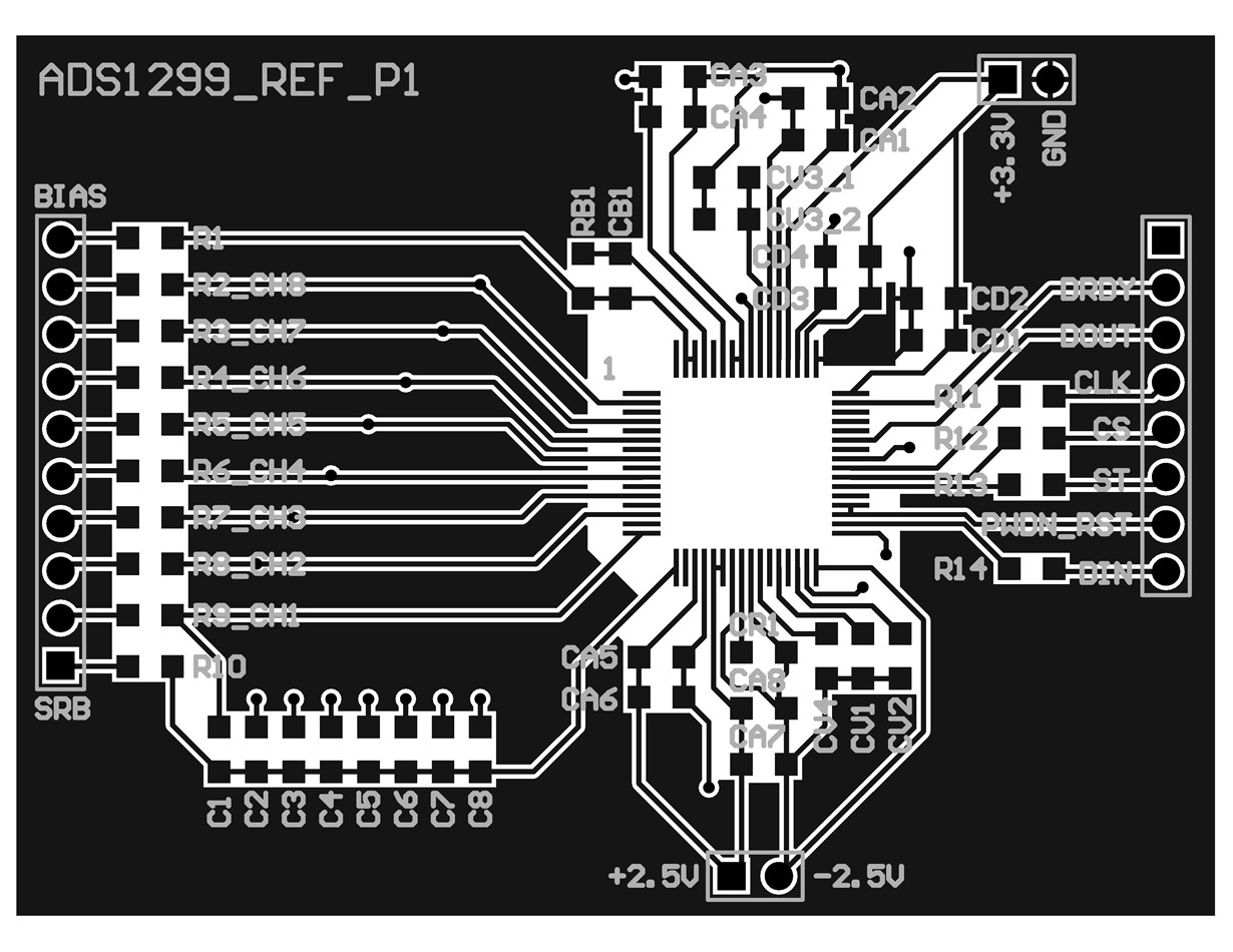
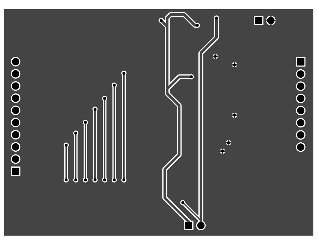
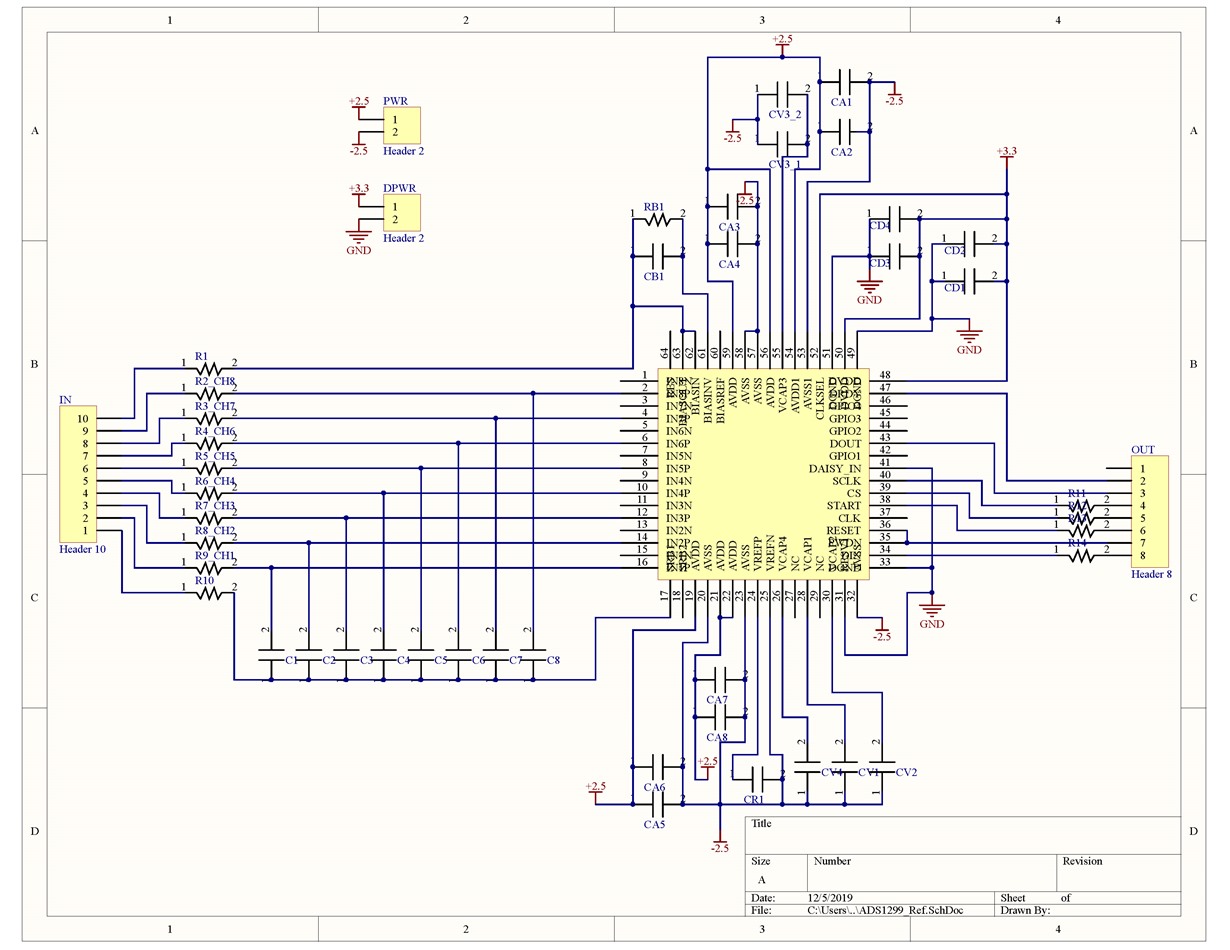
    Below is my schematic and PCB, it's a very simple referential layout, I think I've followed the rules in the datasheet, very much appreciate it if you can have a look.

    Thank you!

    Best,

    Victor

  • Hi Victor,

    My main concern after seeing the schematic and layout are the power supply lines and grounding practices. 

    For example, the DVDD traces in the top right.

    1 line goes directly to pin 52 with no caps

    1 line goes to pin 50 after passing a pair of caps

    1 line goes to pin 48 after passing a pair of caps

    I believe two sets of caps are unnecessary, one pair would be sufficient. The bulk (large) capacitor should be close to the input terminal, and the smaller capacitor should be as close to the pins as possible. You may be able to debug this by soldering the bulk cap directly at the terminal, and find a way to fly-wire the smaller cap in. It's best to minimize the number of power traces used.  

    I have similar concerns with AVDD.

    Lastly, there should be stitching vias to GND to ensure that there is not excess charge on the planes, especially between the +/-2.5V traces on the bottom of the board. 

    Take a look at the user's guide for the EVM for an example schematic and layout. 

  • Dear Smith,

    Thank you very much for pointing out the problems!

    I'm not experienced in PCB design so I guess I'll learn more about it and try to improve the design.

    Best Regards,

    Victor