This thread has been locked.

If you have a related question, please click the "Ask a related question" button in the top right corner. The newly created question will be automatically linked to this question.

ADS8588S: ADS8588S - Analog and Digital Ground Separate while High speed processor based design

Part Number: ADS8588S

Hi TI Team,

I have selected ADS8588S to interface 32 sensor data reading simultaneously and common analog and digital ground throughout the design.

My question is: Will I need to separate Analog and Digital ground for ADS8588S for processor based high speed design which also have same ground? I have followed EVK reference and current schematic, Digital and Analog both connected common ground , so will be fine?

Below is the schematic look,

Currently we are in the layout freeze stage so please share your inputs.

Thank you,

Nilav Choksi

  • Hi Nilav,

    Splitting analog and digital ground planes is not easy for engineers in some systems with a complex circuitry because the analog and digital ground planes must be at the same potential joined together in close proximity to the device. Hence, using a single solid ground plane is strongly recommended. The EVM board has demonstrated this design to achieve the best performance.

    Regards,

    Dale

  • Hi Dale,

    Thank you for your quick response.

    I have one more question:

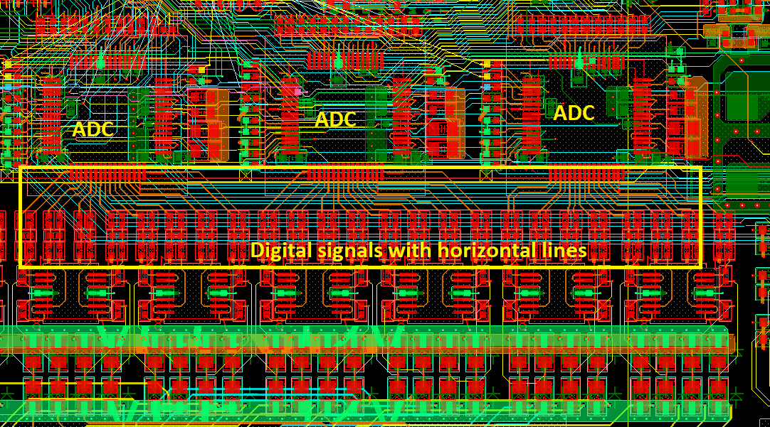
    I am designing 8 layer PCB  and I almost complete routing. But due to space and Layer constraint, I routed digital signals in L3 and L6 layer below Analog section as per image so will it create any issue?

    Note: Analog ADC associated parts are in bottom layer side and routed digital signals(like SPI, I2C and Digital GPIOs) in L3 and L6 with Ground reference(L2 and L7).

    Please share your inputs in this.

    Thank you,

    Nilav Choksi.

  • Hi Nilav,

    I can not predict an issue. However, it's good if your L2 and L7 are dedicated ground planes.

    Regards,

    Dale